.webp)
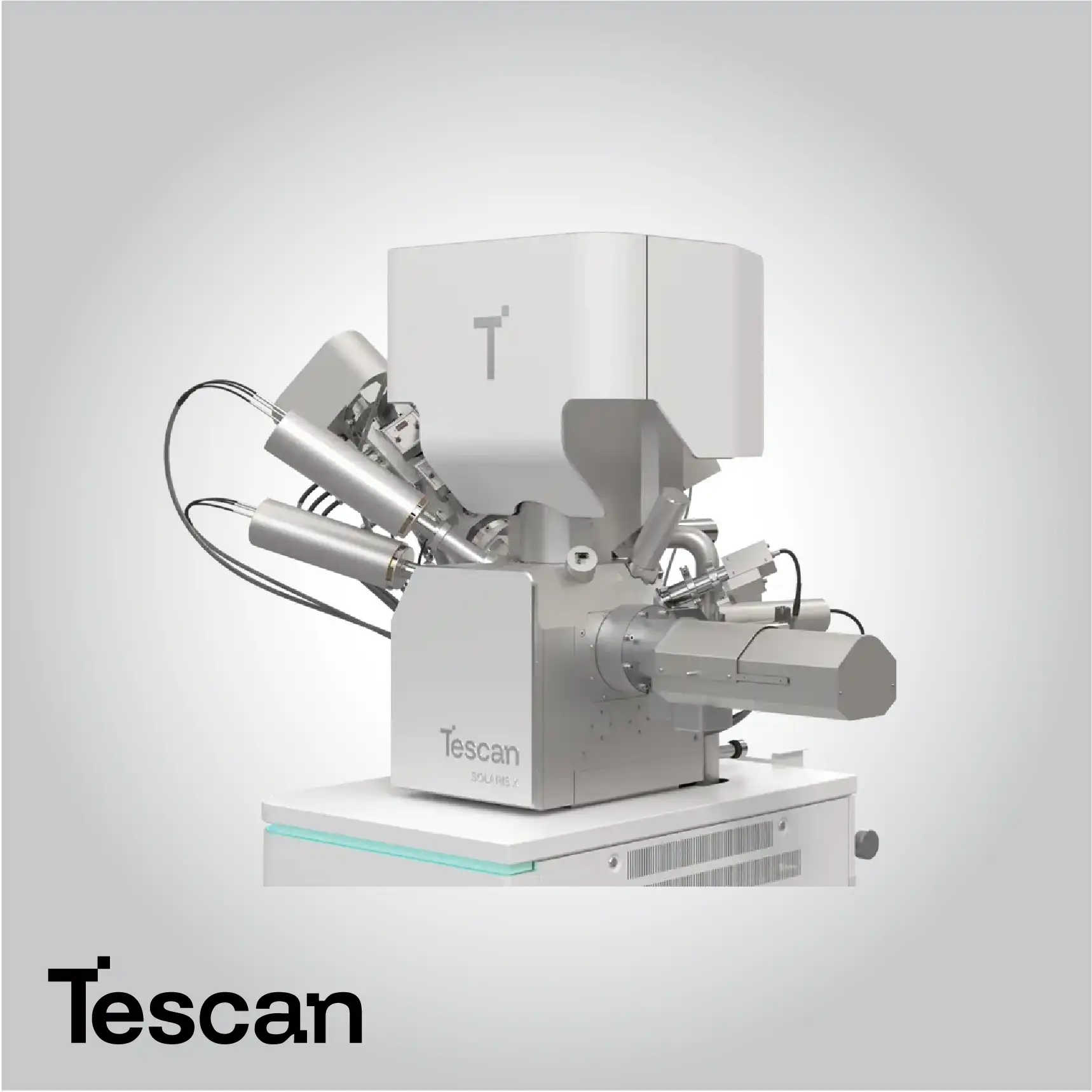
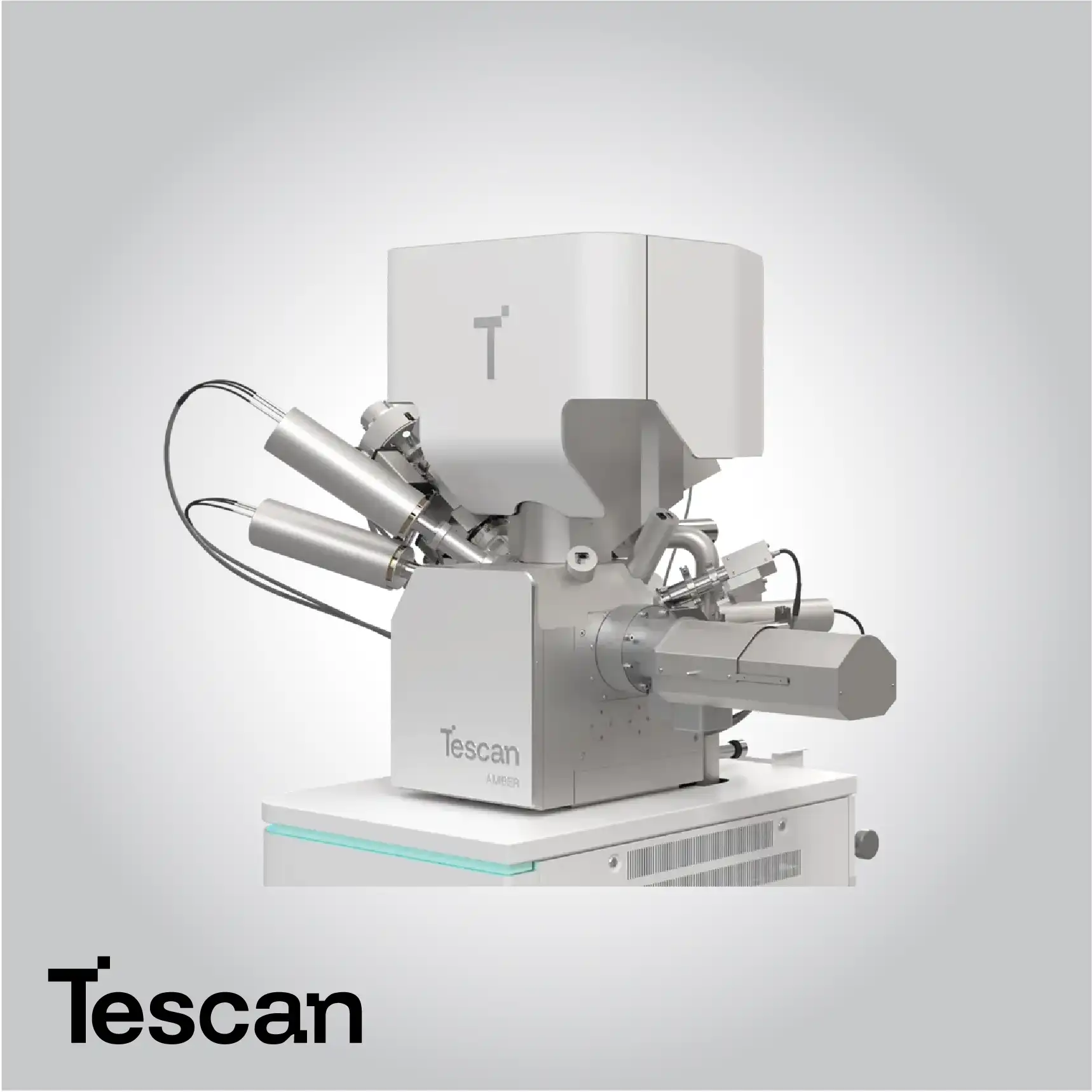
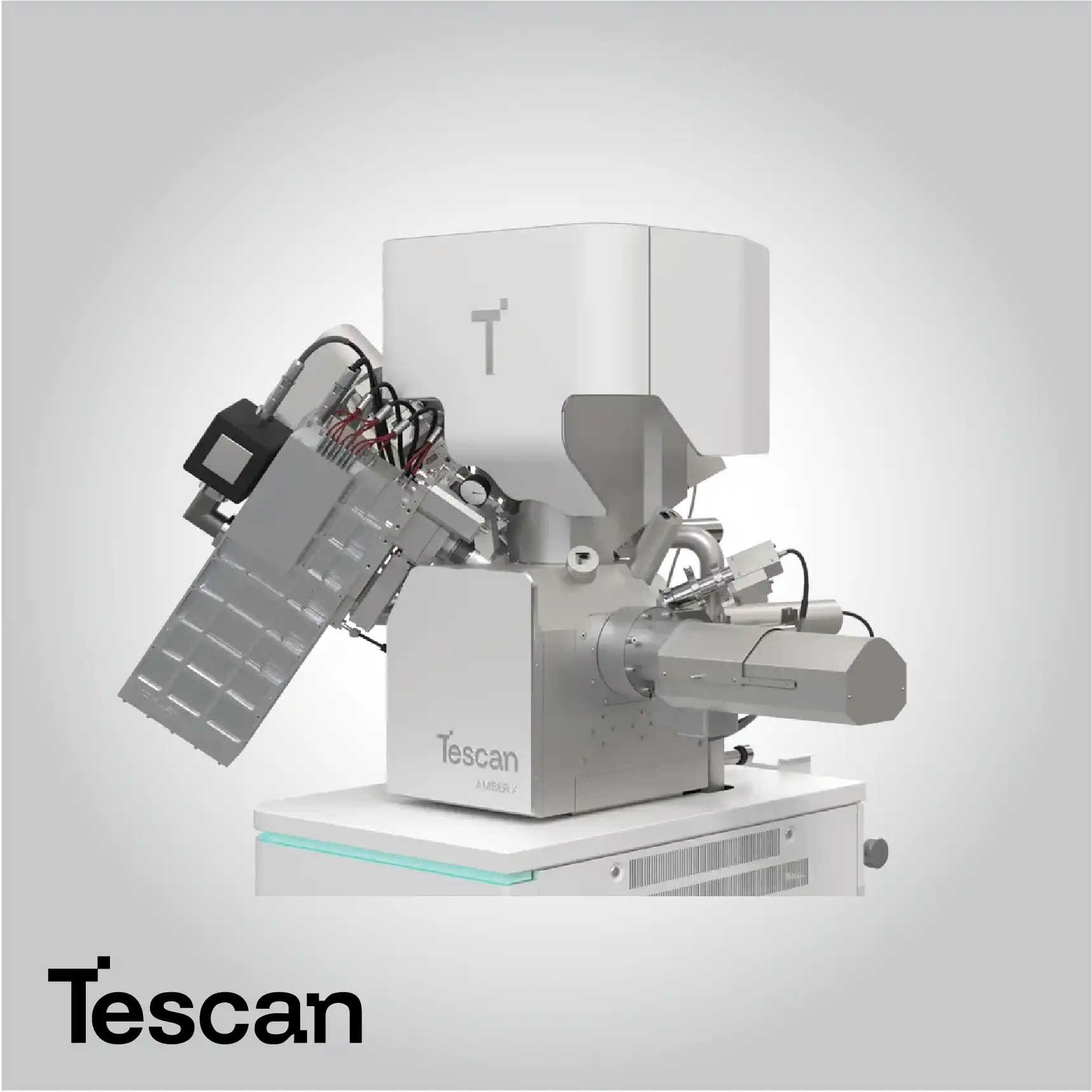
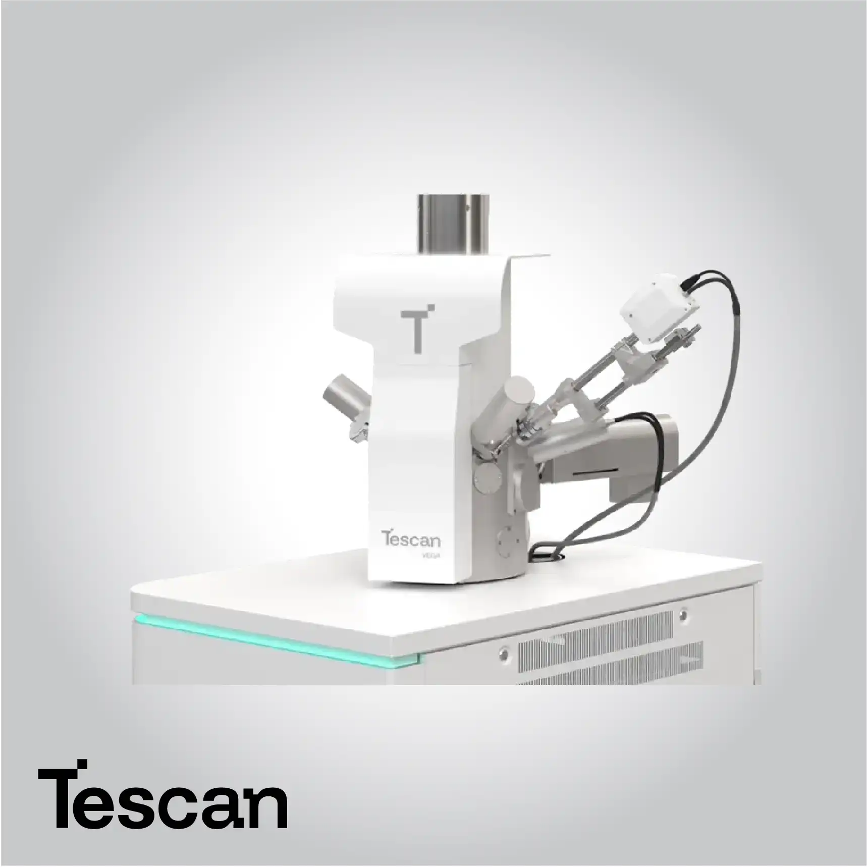
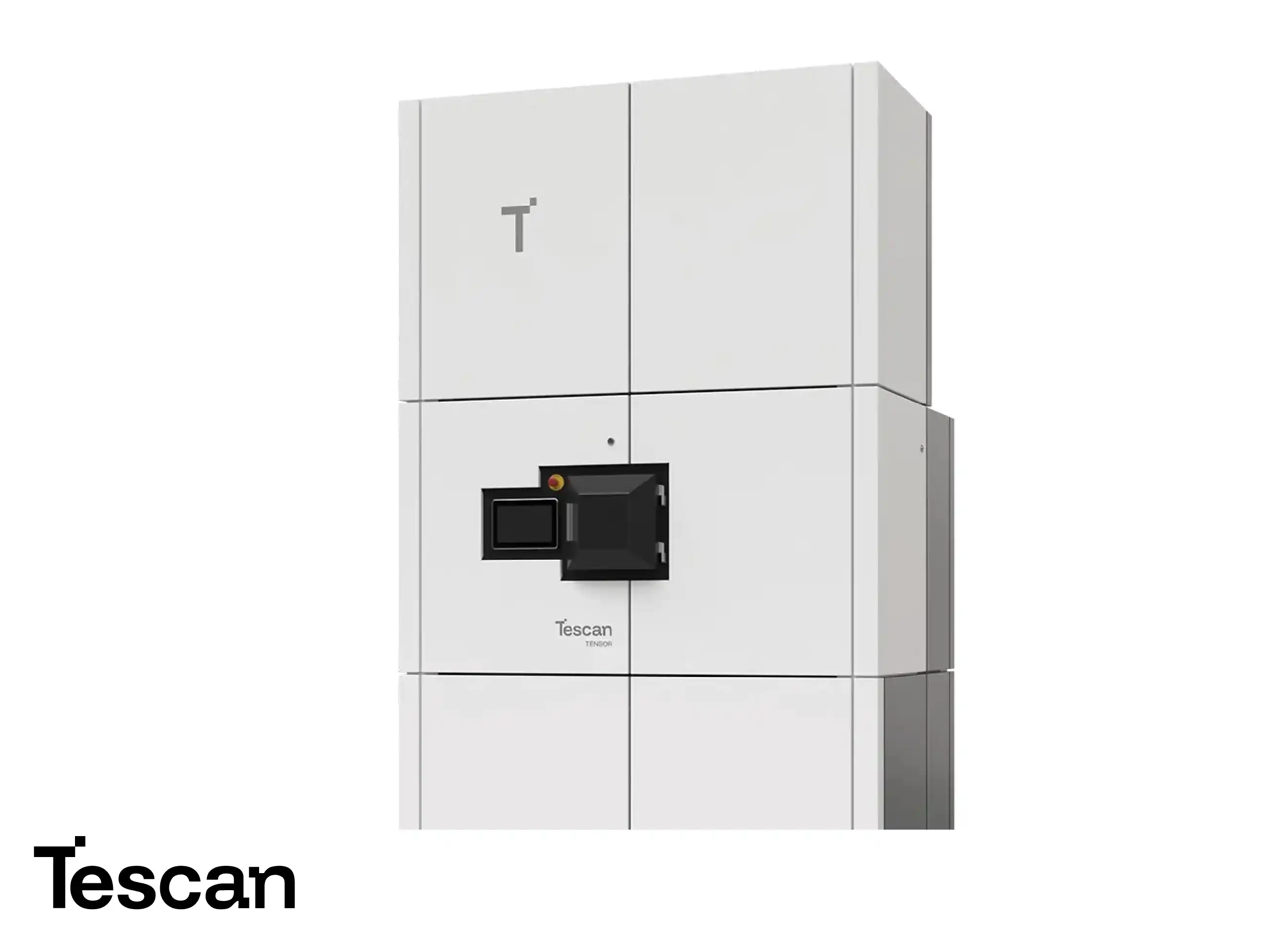
Tescan TENSOR 4D STEM
|
Cutting-Edge STEM Electron Microscopy for Nanostructure Analysis
Tescan 4D STEM
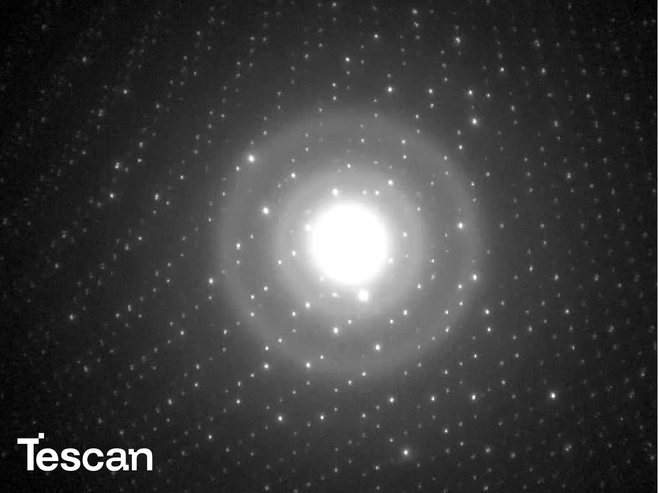
Tescan STEM platforms deliver atomic-scale imaging capabilities that allow direct observation of lattice structures, crystallographic orientations, interfaces, and point defects with sub-nanometer resolution. Advanced electron optics and integrated detectors provide exceptional image contrast, enabling detailed studies of metals, ceramics, semiconductors, and composite materials. Researchers can investigate grain boundaries, dislocations, and phase transitions with high precision, while capturing subtle structural variations that influence material performance.
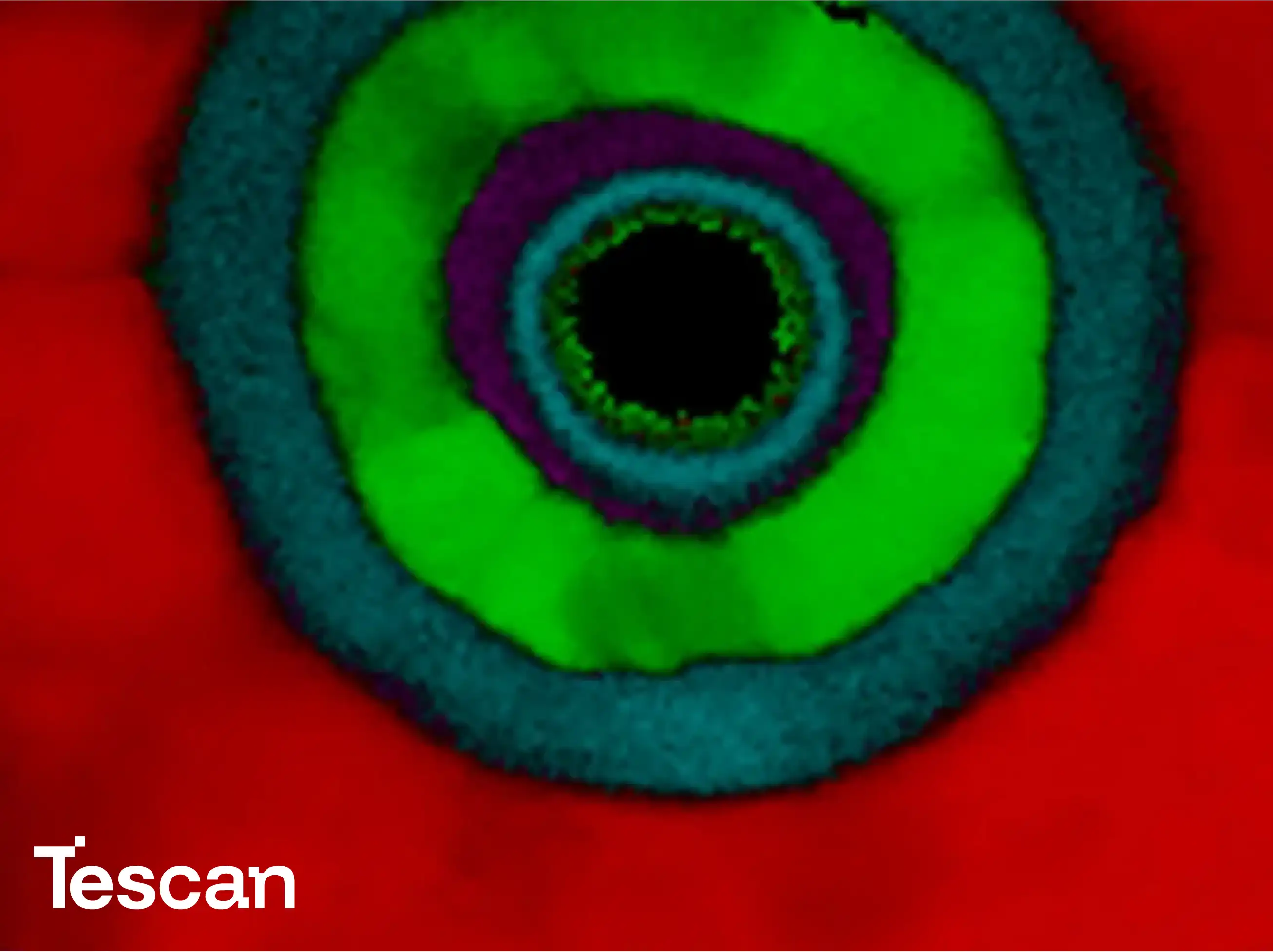
In addition to imaging, Tescan STEM systems incorporate advanced analytical detectors that enable simultaneous elemental mapping, energy-dispersive spectroscopy (EDS), and other chemical analysis techniques. This integrated approach allows precise microanalysis of nanostructures, providing quantitative information about chemical composition, heterogeneity, and localized elemental distributions. Researchers can correlate structural and chemical data, facilitating a comprehensive understanding of complex materials, evaluating their performance under various conditions, and optimizing material design for industrial or research applications.
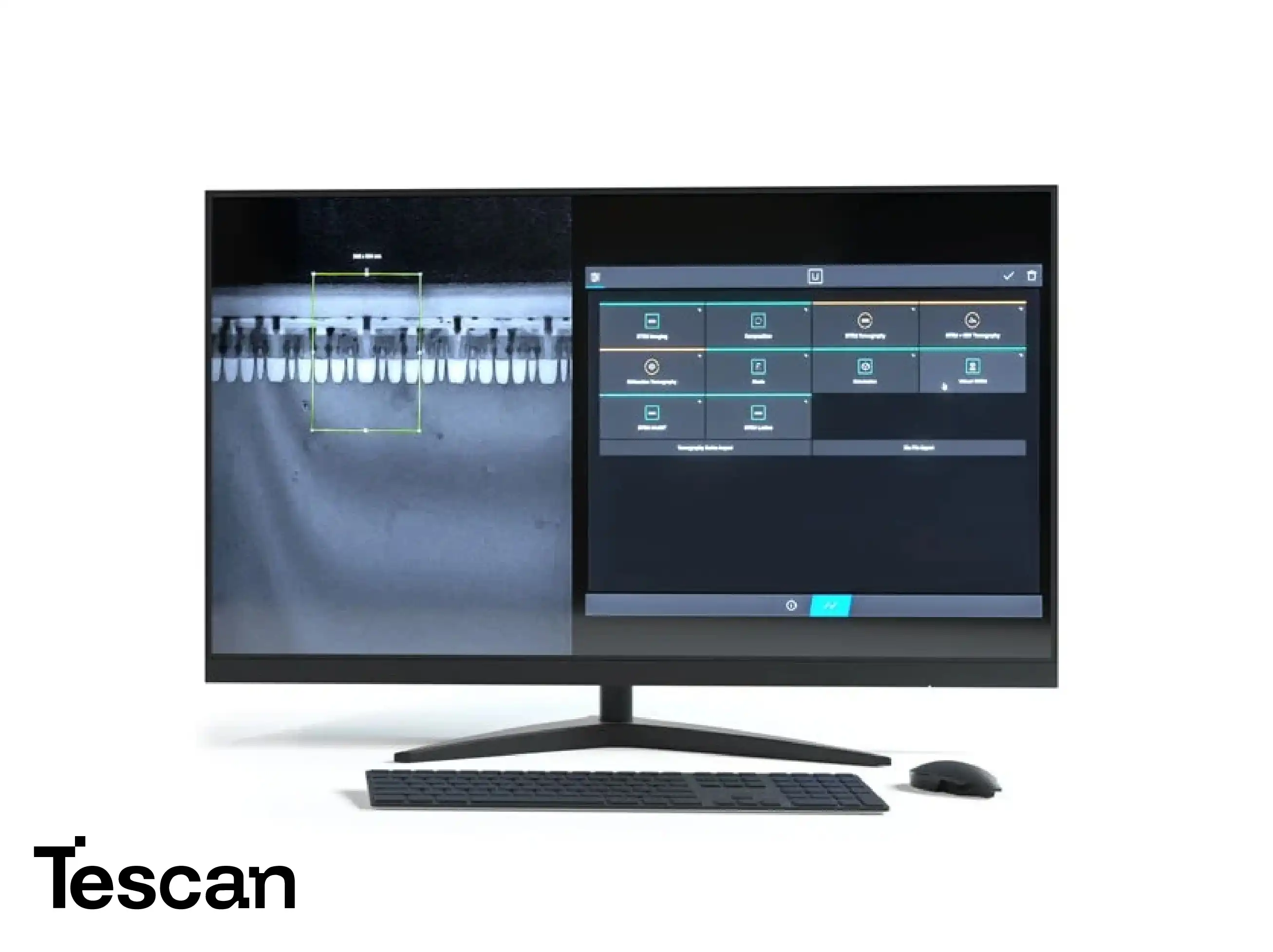
Sample Preparation, Automation, and Workflow Optimization
TESCAN STEM systems feature fully integrated sample preparation workflows, including lamella preparation for TEM analysis, automated stage control, and precise beam alignment. These capabilities reduce user variability and increase reproducibility, ensuring consistent high-quality imaging and analysis across multiple experiments. Automated processes streamline complex procedures, saving time and improving efficiency for laboratories conducting high-volume or high-precision research.
Nanostructure Characterization and Morphology Analysis
Advanced STEM systems allow detailed visualization and characterization of nanoscale structures, such as nanoparticles, nanowires, quantum dots, and layered nanocomposites. High-resolution imaging combined with analytical detectors enables accurate measurement of size, shape, morphology, and chemical composition, facilitating the design of novel nanomaterials and the study of their functional properties.
Defect and Interface Analysis
STEM provides precise tools for analyzing defects, interfaces, and heterostructures within complex materials. Researchers can identify vacancies, dislocations, grain boundaries, and phase transitions, which are critical for understanding mechanical, electronic, and chemical behavior. Detailed interface analysis supports studies in semiconductor devices, composites, and nanoscale engineering applications.
Crystallography and Phase Mapping
STEM enables high-precision crystallographic studies, allowing determination of lattice parameters, crystal orientation, and phase distribution within heterogeneous materials. The system supports advanced phase mapping and orientation imaging, facilitating investigations of microstructural evolution, strain, and phase transformations in metals, ceramics, and other crystalline materials.
Spectroscopy and Elemental Mapping
Integrated analytical modules provide energy-dispersive spectroscopy (EDS), electron energy loss spectroscopy (EELS), and other elemental mapping techniques. This combination allows simultaneous acquisition of structural and chemical data, enabling precise correlation of material composition with morphological and crystallographic features. Such capabilities are essential for materials research, nanotechnology, and failure analysis applications.
Correlative Microscopy and Multimodal Studies
STEM systems can be combined with complementary imaging modalities for correlative studies, allowing integration of structural, chemical, and functional information. Multimodal analysis provides a holistic view of complex samples, from nanostructured materials to biological specimens, supporting interdisciplinary research and advanced analytical workflows.
High-Throughput Analysis and Data Reproducibility
Automation and advanced software enable high-throughput imaging and analysis, allowing multiple samples to be processed efficiently with minimal operator intervention. Reproducible workflows enhance data reliability, streamline experiments, and accelerate research productivity in academic and industrial laboratories.
Applications in Research and Industry
TESCAN STEM platforms serve as essential tools for both academic research and industrial applications, including nanotechnology, materials engineering, semiconductor development, and composite material analysis. Their combination of atomic-scale imaging, integrated chemical analysis, and advanced automation provides flexibility, precision, and reliability for cutting-edge scientific investigations.
Read more about Tescan products here