.webp)
Home » Products » Scanning Electron Microscopy » Scanning Electron Microscopy - SEM » Tescan Material Science SEM
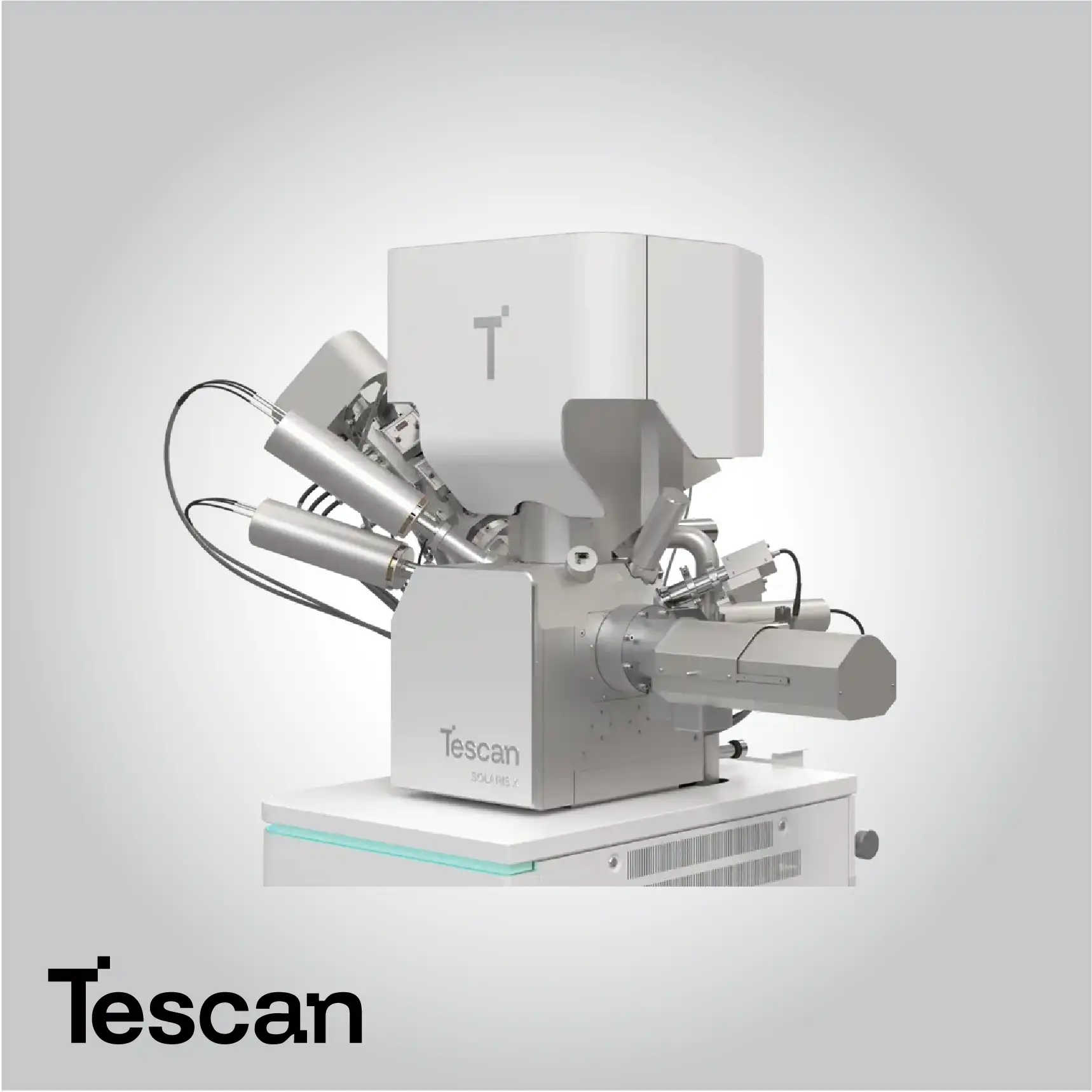
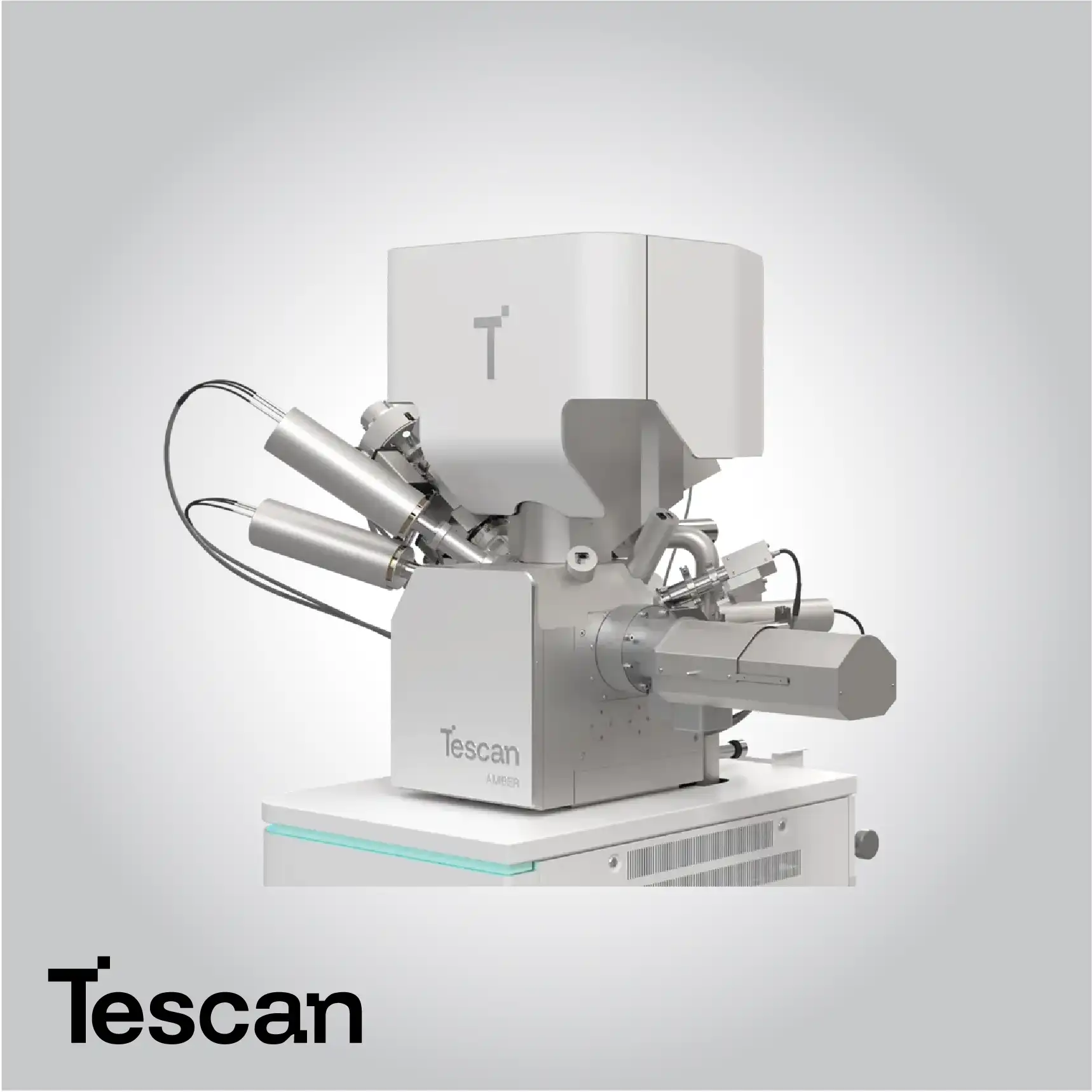
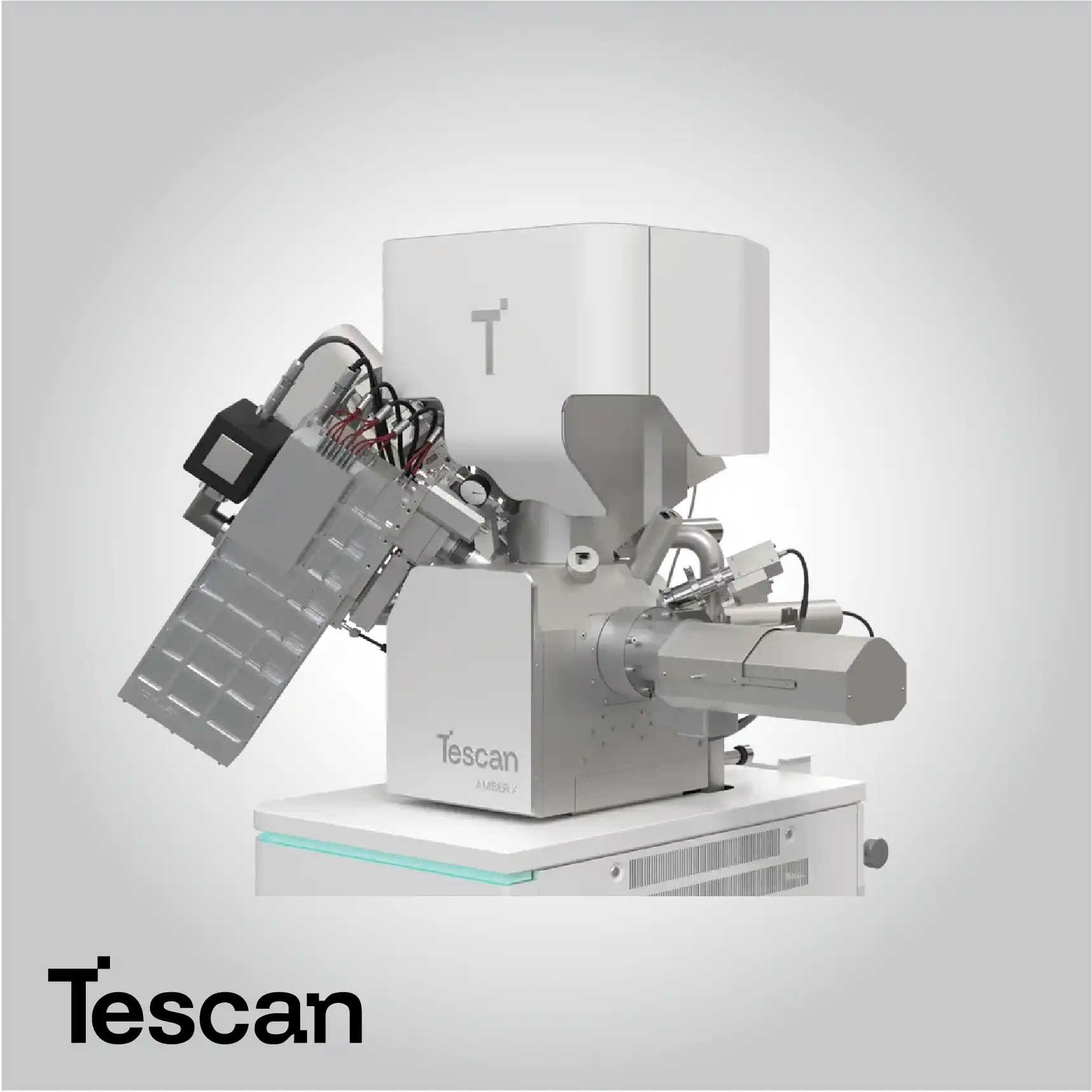
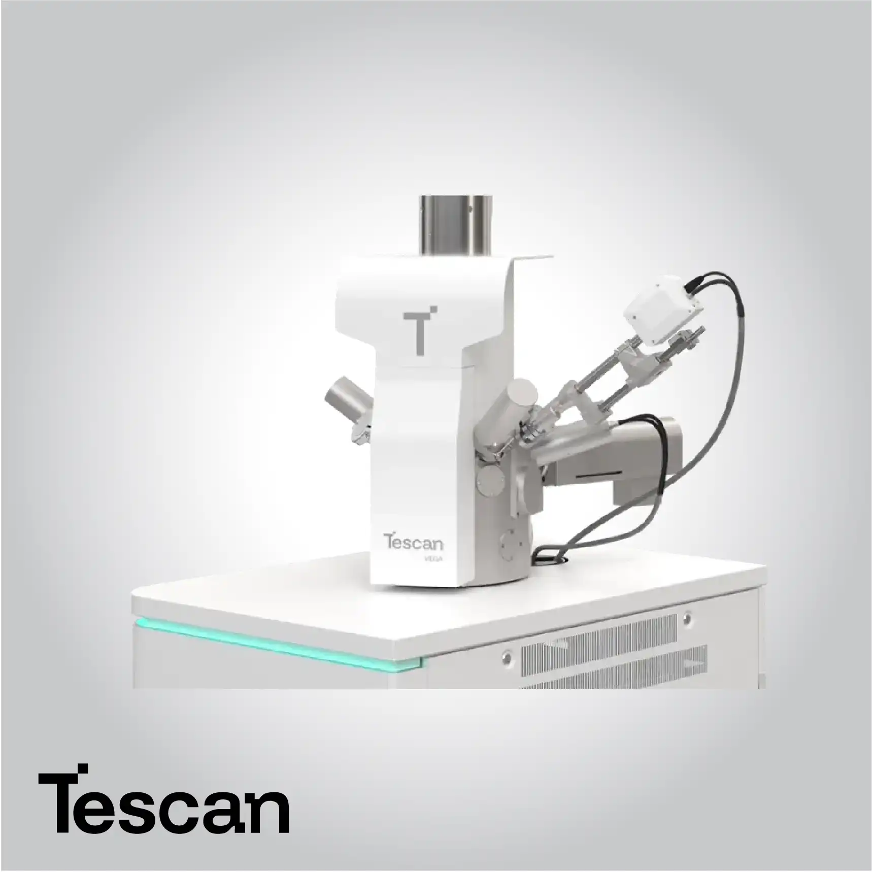
Tescan Material Science SEM
|
TEScan Scanning Electron Microscopes for Material Science
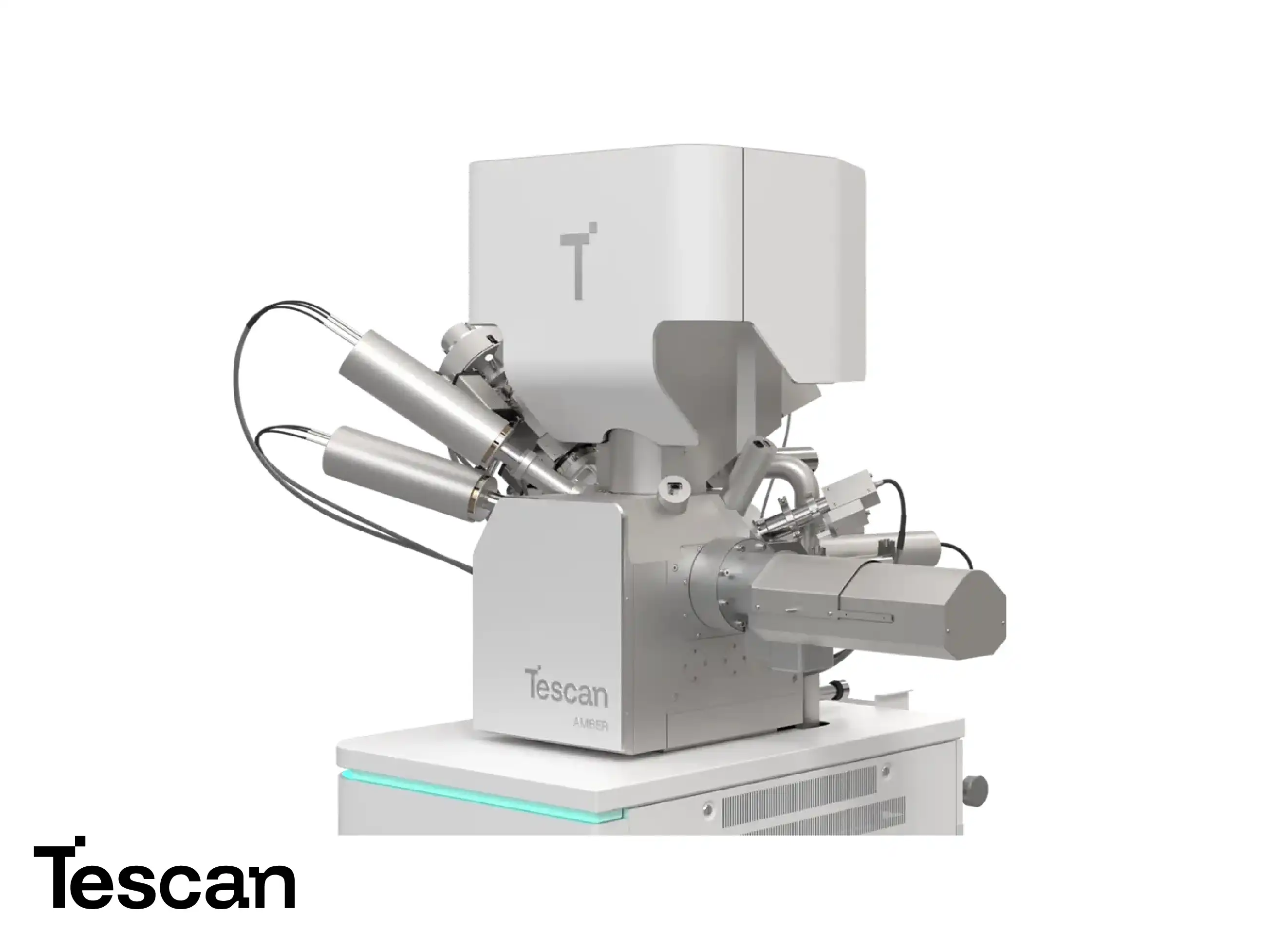
Tescan Material Science SEM
TEScan Scanning Electron Microscopes for Material Science deliver precision, flexibility, and analytical power for comprehensive materials characterization. They are designed to reveal the finest details of metals, ceramics, polymers, composites, and nanomaterials through high-resolution imaging and advanced analytical capabilities. With optimized electron optics, stable beam control, and integrated detectors, these SEM systems provide reliable surface and structural information that supports research, quality assurance, and industrial development.
Engineered for both academic and industrial applications, TEScan SEM systems allow users to analyze morphology, composition, and microstructure with exceptional accuracy. They combine imaging versatility with advanced electron beam performance to deliver consistent, artifact-free results. From surface topography to submicron defect detection, TEScan SEM instruments provide comprehensive insight into material behavior and performance, enabling innovation across multiple scientific and engineering disciplines.
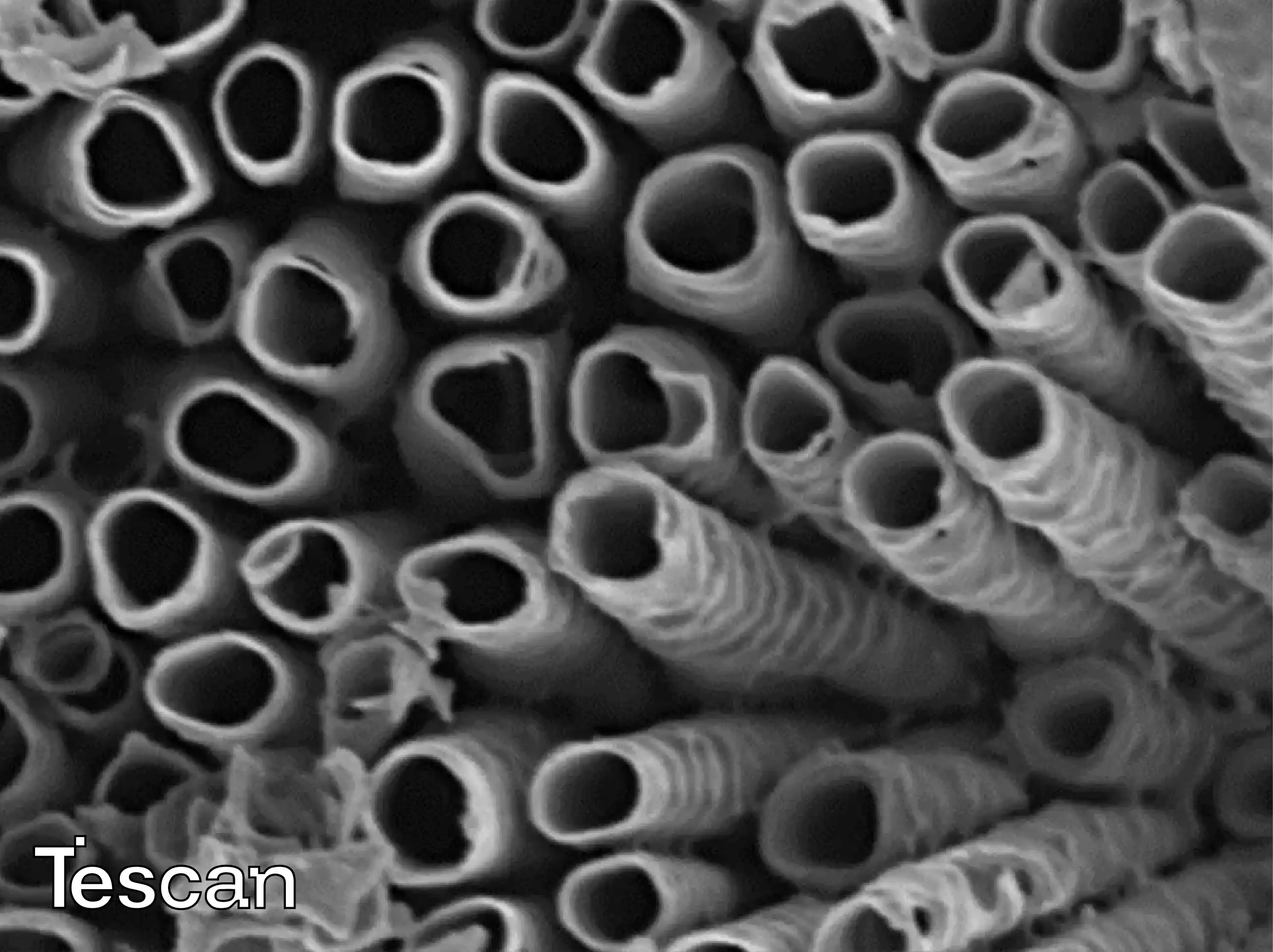
High-Resolution Surface Imaging
TEScan SEM systems provide exceptional imaging quality that reveals the micro- and nano-scale features of material surfaces. Optimized electron beam optics and stable vacuum conditions ensure precise visualization of surface textures, grain boundaries, and phase distributions. This high-resolution capability supports detailed investigation of morphology, coatings, and structural integrity, enabling researchers to understand material performance under various conditions.
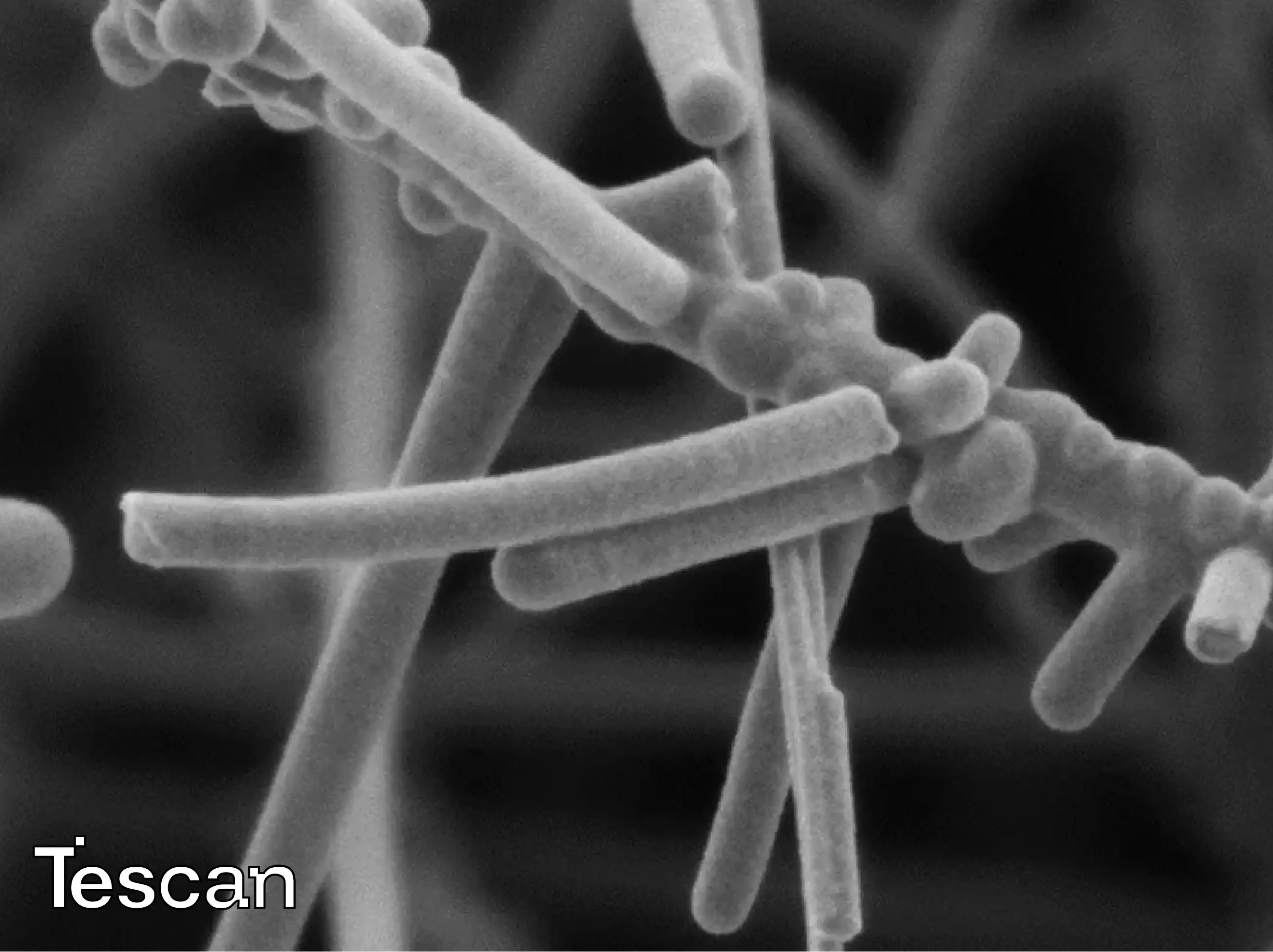
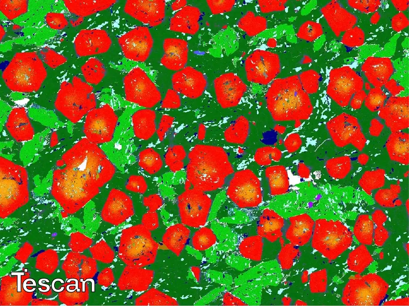
Microstructure and Phase Analysis
TEScan SEM enables the analysis of microstructural components such as grains, inclusions, and interphases. The combination of imaging and analytical signals allows researchers to identify material phases and study relationships between microstructure and mechanical or thermal behavior. This capability is essential for understanding failure mechanisms, improving processing methods, and optimizing material design.
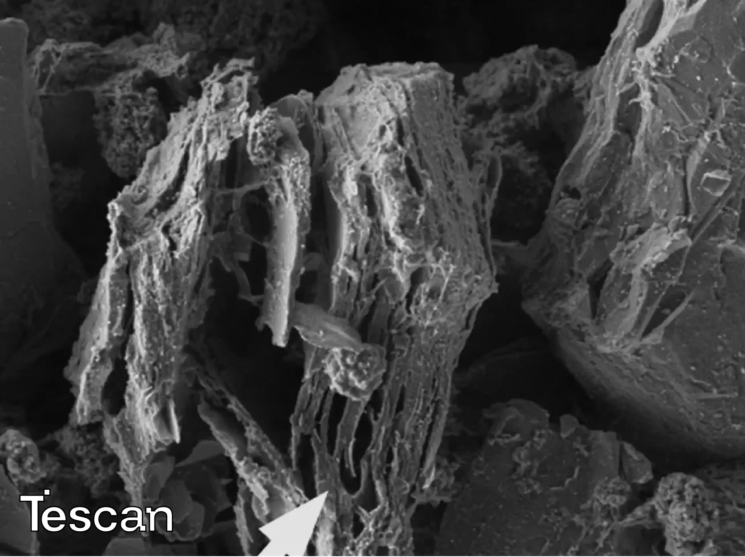
Failure and Defect Investigation
TEScan SEM systems are powerful tools for detecting and characterizing surface and subsurface defects. High-resolution imaging combined with precise depth profiling enables the identification of cracks, voids, and delamination in complex materials. These analyses support quality control processes, reliability testing, and root-cause investigations in industrial and research environments.
Advanced Electron Beam Stability
TEScan SEM features advanced electron beam stability, ensuring consistent imaging and analytical precision over long operation times. The robust column design minimizes drift and distortion, providing accurate image alignment and reproducible measurements. This stability is crucial for time-dependent studies, serial sectioning, and comparative material characterization.
Analytical Flexibility and Integration
TEScan SEM instruments support integration with multiple analytical tools, expanding capabilities for comprehensive materials characterization. Techniques such as energy-dispersive spectroscopy (EDS) or 3D surface reconstruction can be combined to provide elemental, structural, and topographical data in a single workflow. This integration enhances understanding of material composition and functional properties.
Versatility Across Material Types
TEScan SEM systems accommodate a wide range of material types, from metals and ceramics to polymers, composites, and nanostructures. The adjustable chamber configurations and variable pressure modes enable imaging of both conductive and non-conductive specimens. This versatility ensures that the same platform can serve research and production environments alike.
Quantitative and Correlative Analysis
TEScan SEM supports quantitative imaging workflows, enabling measurement of particle size, distribution, and surface roughness. In addition, correlative analysis connects SEM data with complementary imaging techniques, providing a multi-scale view of material structure and properties. This approach enhances accuracy in evaluating complex materials and processes.
Reliability for Research and Industry
Built for demanding laboratory and production settings, TEScan SEM systems deliver long-term reliability and consistent analytical performance. The robust design and intuitive software interface streamline workflows and minimize downtime. Researchers and engineers benefit from dependable data acquisition that supports both innovation and quality control in materials science.
Read more about Tescan products here
.webp)
.webp)
.webp)