Home » Products » Scanning Electron Microscopy » Focused Ion Beam-Scanning Electron Microscopes (FIB-SEM) » Tescan FIB-SEM for Semiconductors
Tescan FIB-SEM for Semiconductors
|
High-Precision Cross-Sectioning and Nanoscale Process Analysis
Tescan FIB-SEM for Semiconductors
Tescan FIB-SEM systems for semiconductor applications deliver precision cross-sectioning, imaging, and analysis tailored to advanced micro- and nanoscale devices. By combining focused ion beam milling with high-resolution SEM imaging, these systems allow researchers and engineers to visualize internal layers, interfaces, and defects within semiconductor wafers, thin films, and complex integrated circuits. The controlled ion beam removes material with nanometer precision, producing smooth surfaces that are ideal for structural inspection and compositional analysis.
These FIB-SEM systems integrate high-speed ion beam control, automated workflows, and analytical tools to facilitate process development and failure analysis. Users can perform 3D reconstruction of semiconductor layers, investigate defects, and study layer interfaces in detail. The platform supports multi-modal imaging, volumetric analysis, and site-specific sample preparation, enabling researchers to link microstructural features with electrical, thermal, or mechanical performance. With precise beam control, minimal sample damage, and reproducible results.
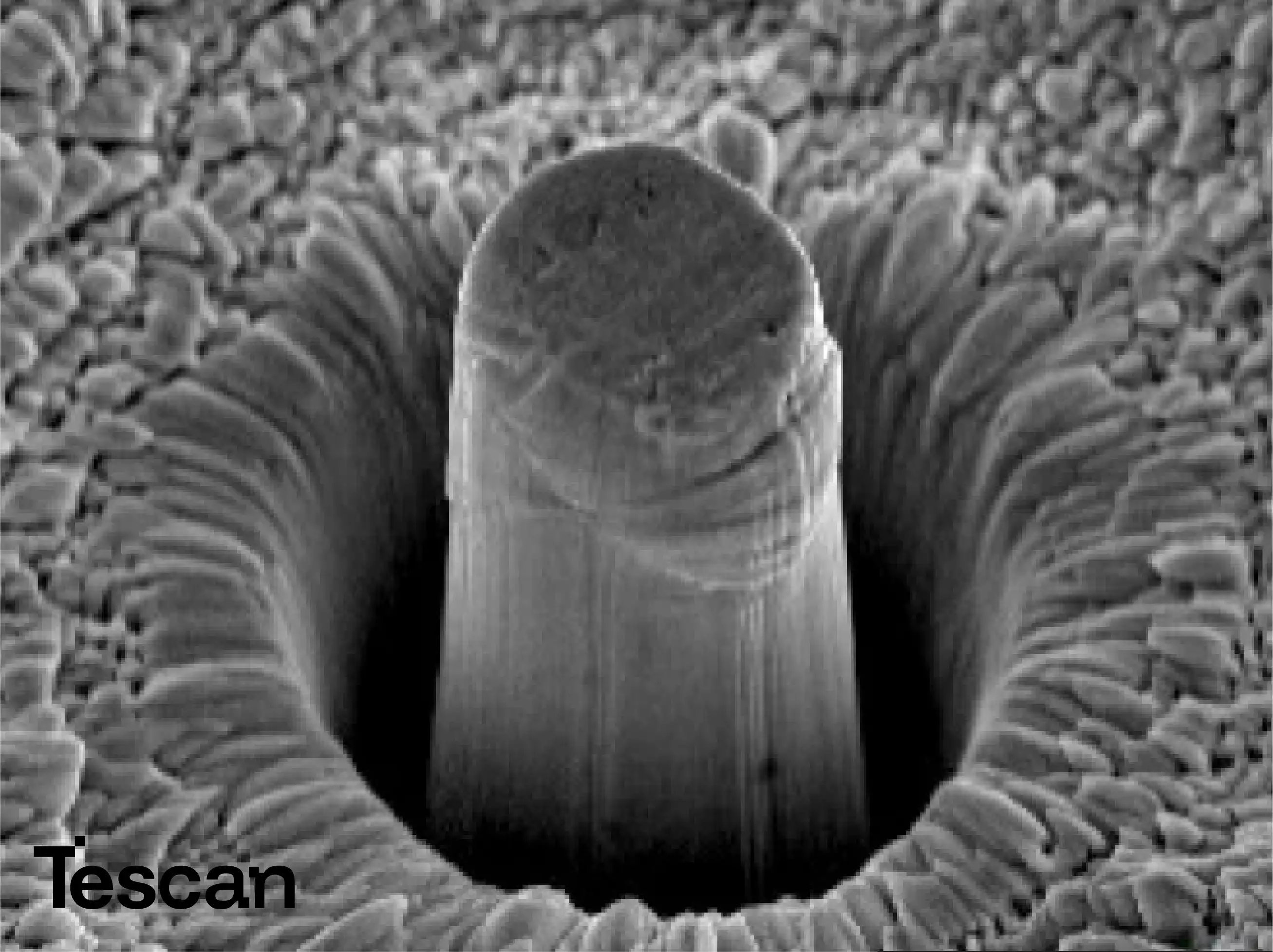
Site-Specific Cross-Sectioning for Semiconductor Devices
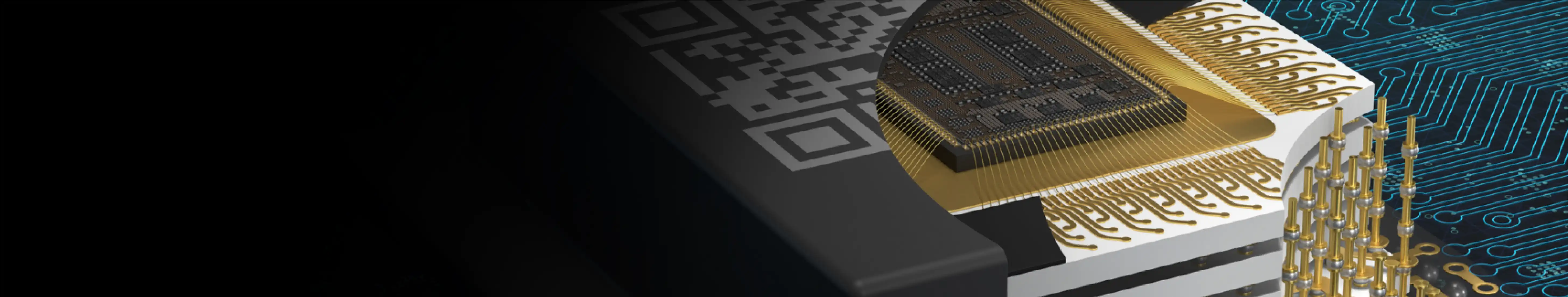
Tescan FIB-SEM systems offer unmatched precision for site-specific cross-sectioning of semiconductor devices. Using a focused ion beam, the system mills target regions at nanometer-scale accuracy, exposing internal features such as transistor gates, interconnects, and thin films without introducing mechanical stress or artifacts. This controlled material removal enables direct observation of interfaces, buried layers, and defects, providing essential data for device optimization. Furthermore, site-specific lamella preparation facilitates TEM and STEM analysis, allowing researchers to correlate nanoscale features with device performance. By controlling the beam parameters and milling strategy, the system ensures minimal sample damage while delivering reproducible and high-quality surfaces suitable for advanced structural and compositional analysis.
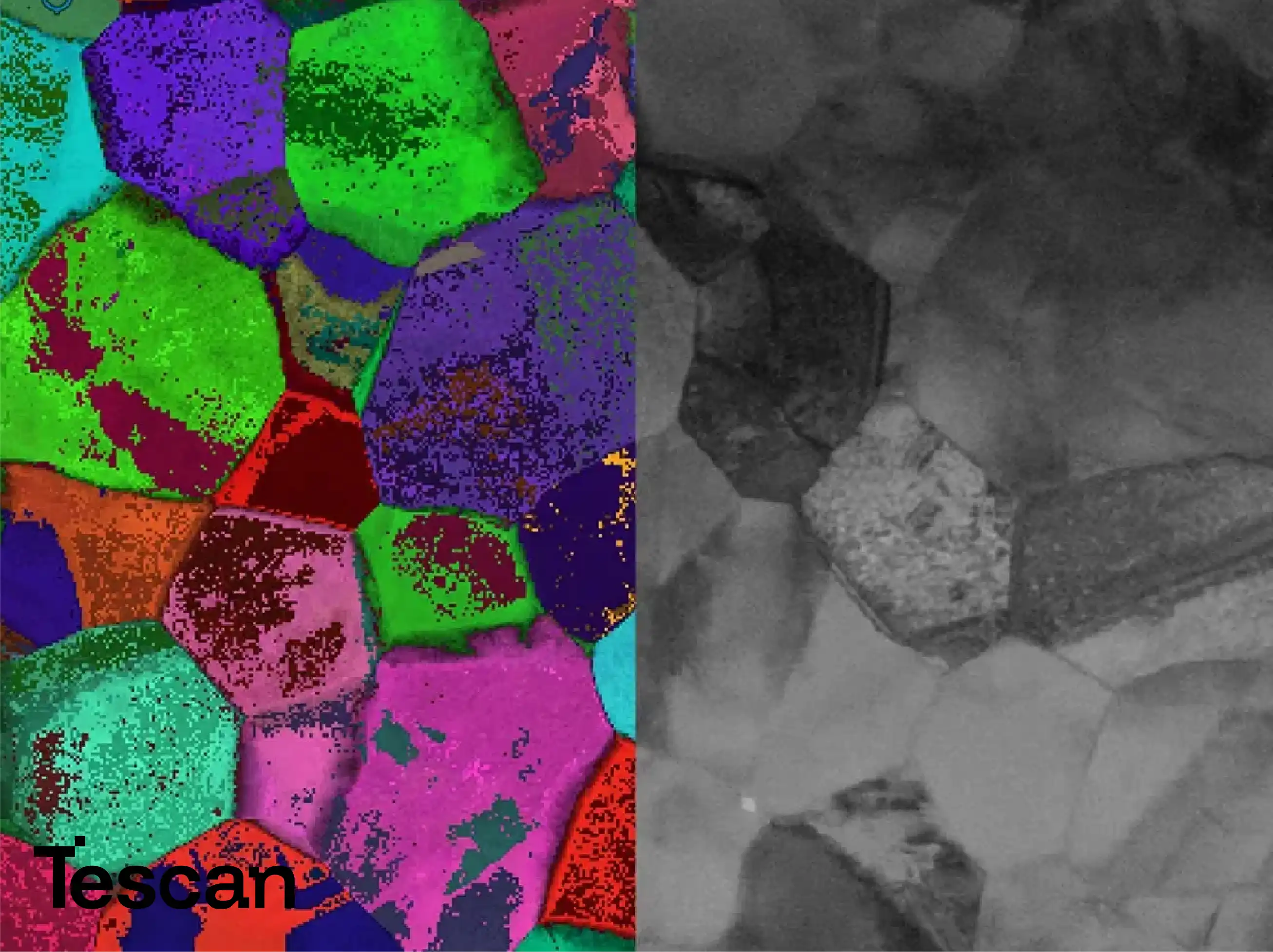
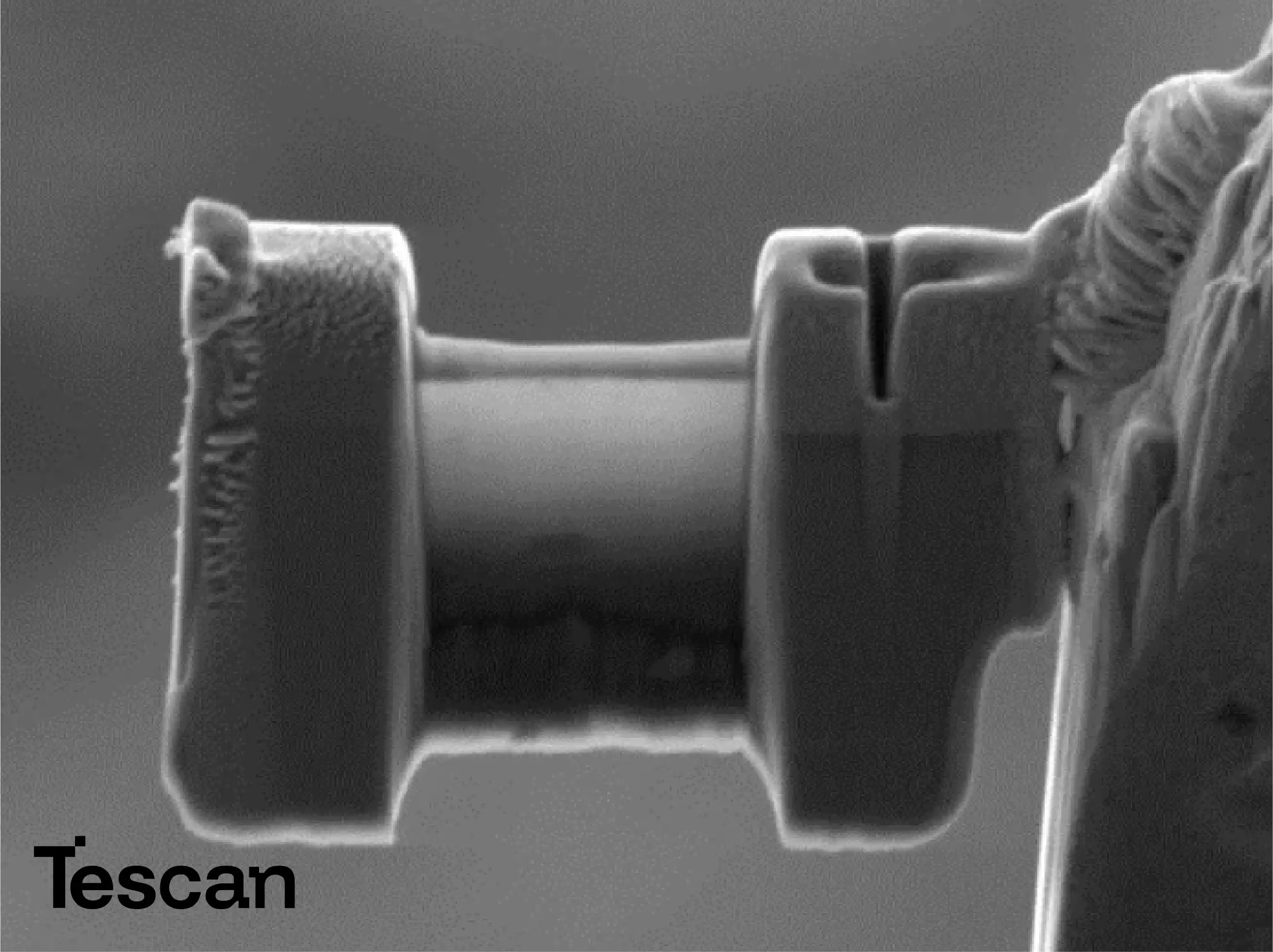
High-Resolution Imaging of Nanoscale Semiconductor Features
Equipped with advanced electron optics and high-sensitivity detectors, Tescan FIB-SEM systems produce exceptionally clear, high-contrast images of nanoscale semiconductor structures. Users can visualize gate electrodes, vias, thin films, metallization layers, and defects with precision previously unattainable in conventional SEM systems. High-resolution imaging allows detailed morphological analysis, helping engineers understand layer uniformity, grain boundaries, and the influence of processing steps on device quality. The stable electron beam ensures minimal drift or charging effects, enabling repeated imaging at the same location for time-resolved studies or defect progression analysis. This imaging capability is critical for both research and production monitoring, ensuring that micro- and nanoscale structures meet stringent semiconductor fabrication standards.
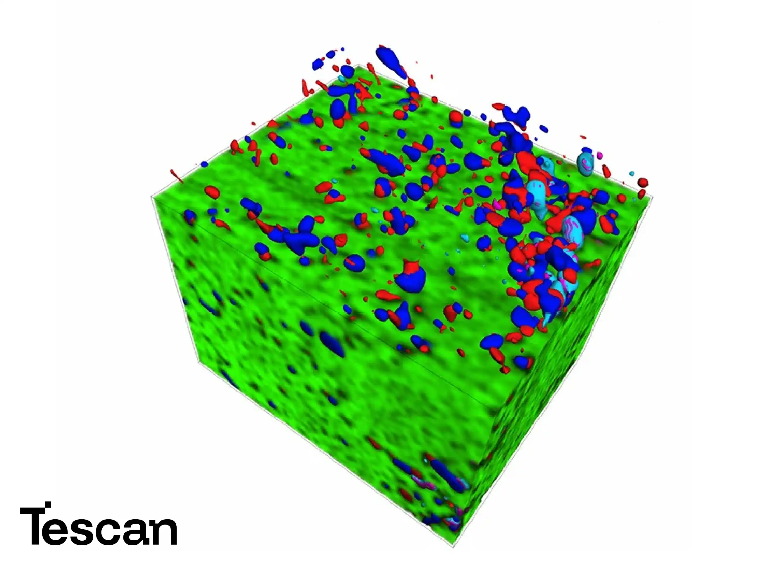
Three-Dimensional Device Reconstruction and Volumetric Analysis
By combining automated serial ion milling with sequential SEM imaging, Tescan FIB-SEM enables high-fidelity 3D reconstruction of semiconductor devices. Researchers can visualize buried interconnects, multilayer structures, and defects in three dimensions, providing insight into layer connectivity, void distributions, and stress propagation. Volumetric datasets can be quantitatively analyzed for layer thickness, porosity, and feature alignment, which is essential for process optimization, failure analysis, and device qualification. The ability to explore the full 3D architecture allows engineers to identify weak points or structural inconsistencies that might impact device reliability, guiding corrective actions during research, development, or industrial manufacturing.
Defect Analysis and Failure Investigation
Tescan FIB-SEM systems enable detailed investigations of structural defects, contamination, delamination, or voids within semiconductor devices. Through precise site-specific milling, critical regions are exposed without introducing new artifacts, allowing high-resolution imaging and analysis. Researchers can study defect propagation, interface delamination, or material inconsistencies to determine root causes of device failure. The platform’s ability to integrate imaging with analytical techniques such as EDS provides additional chemical context, helping identify contamination sources, material diffusion, or phase transformations that affect device performance. This makes FIB-SEM an indispensable tool for reliability testing and advanced failure analysis in semiconductor R&D and production environments.
Integration with Analytical Techniques for Material and Interface Characterization
Tescan FIB-SEM systems can integrate with energy-dispersive X-ray spectroscopy (EDS) and other microanalytical tools to provide elemental and chemical mapping of semiconductor layers and interfaces. This integration allows direct correlation between microstructural observations and chemical composition, which is essential for identifying defects, contamination, or non-uniformity in materials. Researchers can analyze thin-film coatings, diffusion layers, and alloyed regions, helping optimize deposition and etching processes. Combined structural and chemical data provides a comprehensive understanding of device performance, reliability, and manufacturing quality.
Process Development, Quality Control, and Optimization
The precise milling and high-resolution imaging capabilities of Tescan FIB-SEM support semiconductor process development and industrial quality control. Engineers can evaluate deposition uniformity, etching accuracy, and lithography results by directly visualizing cross-sections and 3D volumes of devices. The platform enables feedback for process adjustments, ensuring consistent layer thicknesses, smooth interfaces, and defect-free fabrication. Automated workflows and high reproducibility reduce operator variability and accelerate process optimization, making it an essential tool for improving yield and ensuring compliance with industry standards in semiconductor manufacturing.
Automation and Advanced Workflow Management
TESCAN FIB-SEM systems offer advanced automation features that streamline serial sectioning, imaging, and data collection, reducing operator intervention and increasing efficiency. Automated milling, imaging, and reconstruction workflows allow users to analyze multiple devices or samples consistently and reproducibly. Adaptive pattern recognition algorithms optimize ion beam paths, ensuring precise and repeatable cross-sectioning even in highly complex structures. Automation facilitates high-throughput studies, enables reproducible 3D reconstructions, and frees researchers to focus on data interpretation and decision-making, improving both research productivity and industrial workflow efficiency.
Broad Applications Across Semiconductor Research and Industry
Tescan FIB-SEM systems are versatile tools for microelectronics, MEMS/NEMS devices, power electronics, and advanced semiconductor research. They support characterization of multilayered structures, thin films, and buried interfaces, aiding in process development, device reliability testing, and failure analysis. Their precision, high-resolution imaging, and analytical integration make them indispensable in both academic research and industrial environments. Applications include evaluating metallization, gate structures, interconnects, dielectric layers, and packaging materials. By providing detailed insight into device architecture and defect origins, Tescan FIB-SEM empowers researchers and engineers to improve semiconductor performance, yield, and quality assurance.
Read more about Tescan products here