Home » Products » Scanning Electron Microscopy » Focused Ion Beam-Scanning Electron Microscopes (FIB-SEM) » Tescan FIB-SEM for Material Science
Tescan FIB-SEM for Material Science
|
Precision Cross-Sectioning, 3D Analysis, and Advanced Structural Characterization
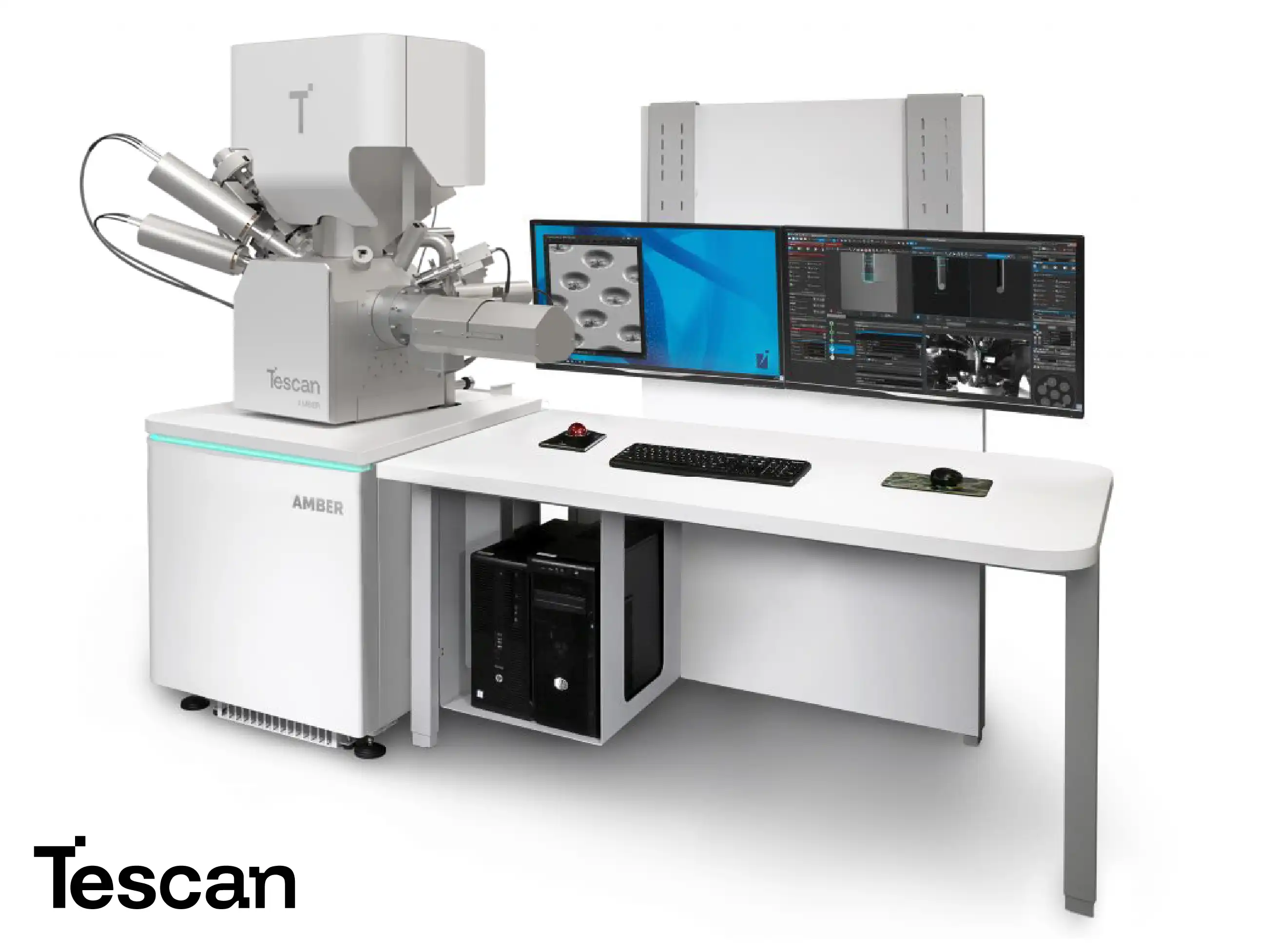
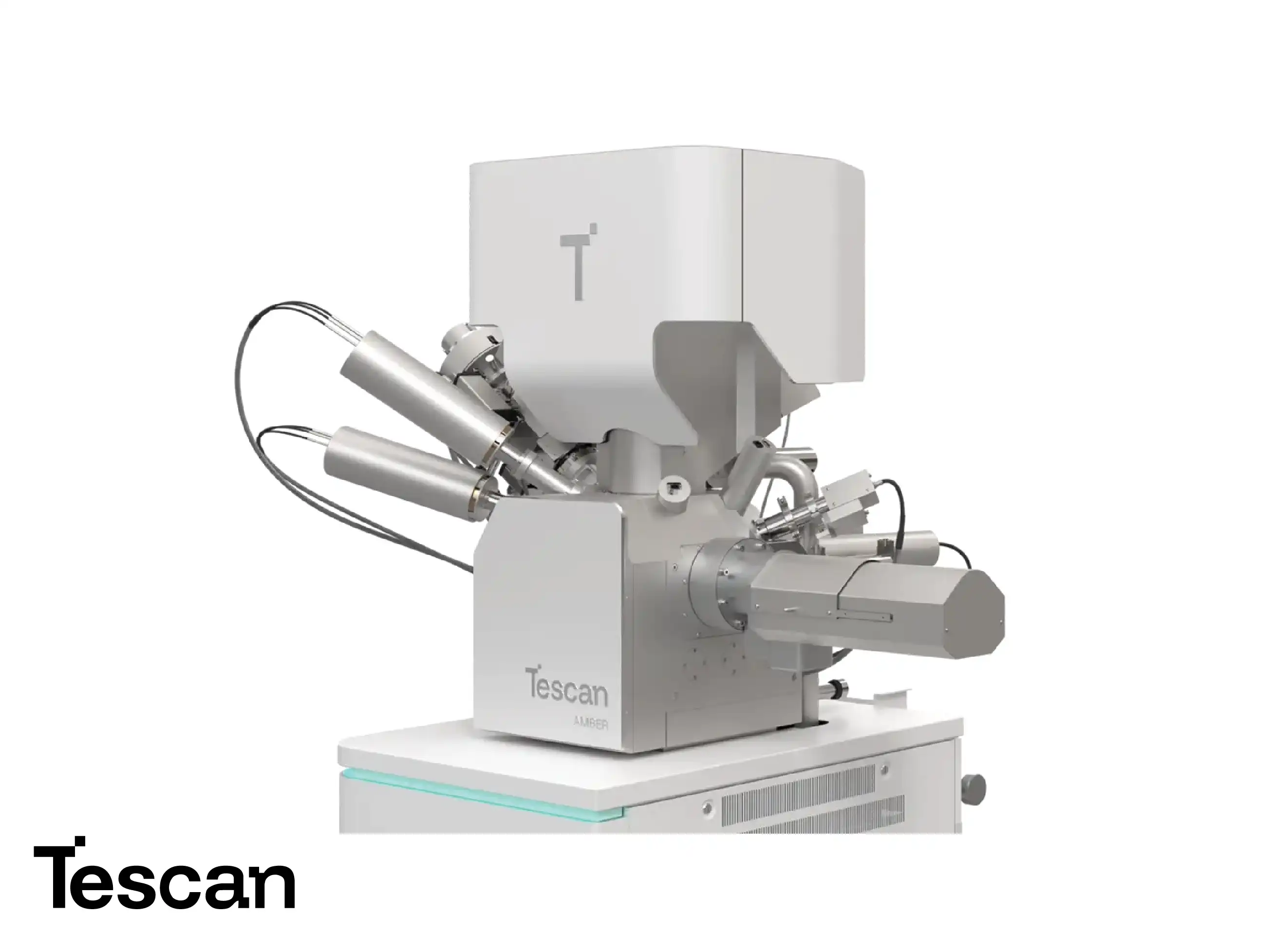
Tescan FIB-SEM for Material Science
Tescan FIB-SEM systems for material science integrate focused ion beam technology with high-performance scanning electron microscopy to enable structural and compositional analysis of materials at the nanoscale. These dual-beam instruments are designed for the detailed study of microstructures, interfaces, and defects, allowing researchers to perform targeted cross-sectioning, imaging, and analytical investigations with sub-micron precision.
Through advanced ion beam control, automated workflows, and analytical integration, Tescan FIB-SEM systems deliver comprehensive insight into the morphology, chemistry, and crystallography of materials. They support applications across metallurgy, semiconductors, ceramics, composites, and energy materials. By enabling high-precision cross-sections, subsurface analysis, and 3D tomography, researchers can visualize grain structures, phase boundaries, and failure mechanisms with unmatched clarity. These instruments form the backbone of modern material science workflows — from academic research to industrial process optimization.
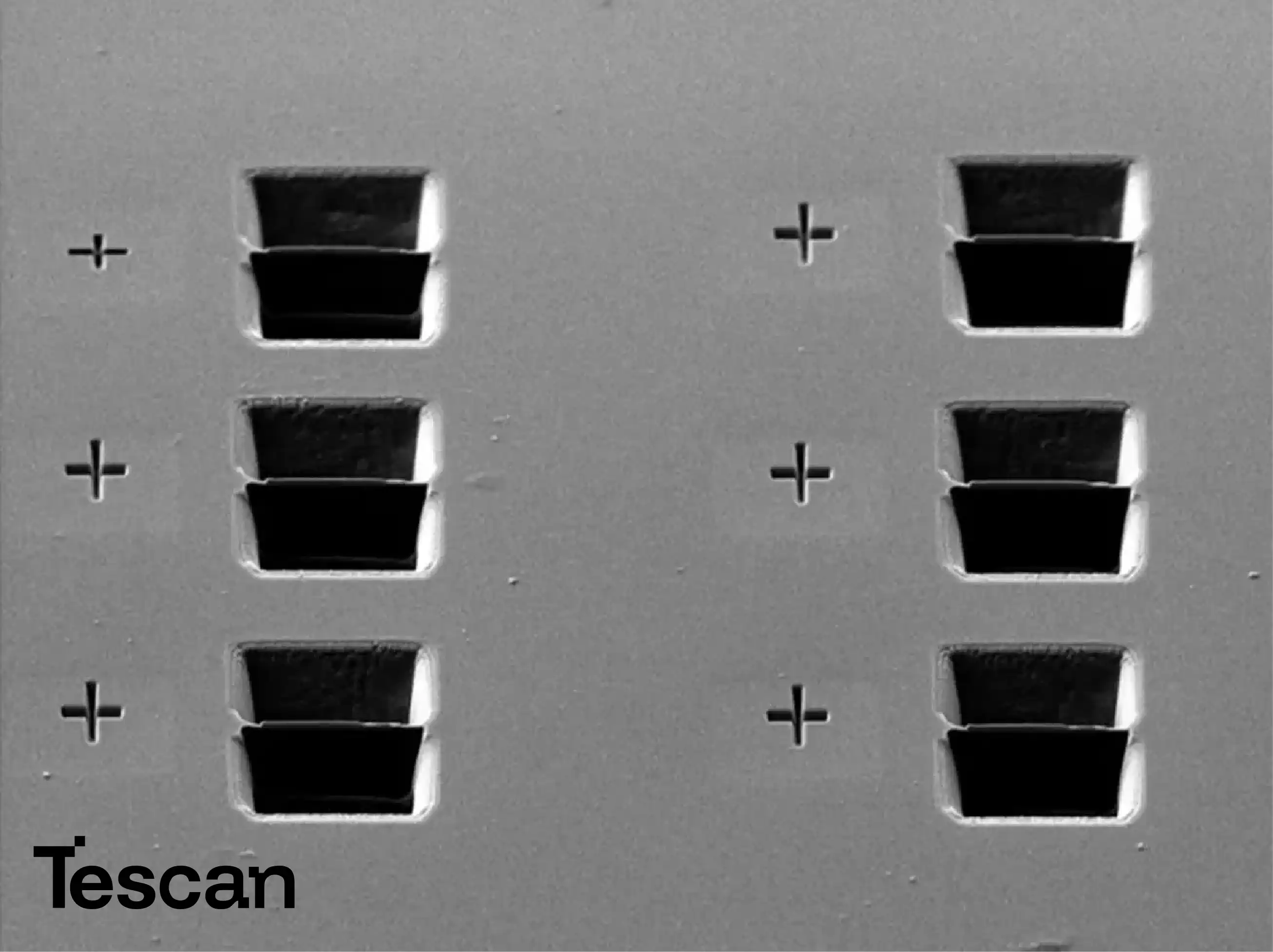
Site-Specific Cross-Sectioning and Precise Sample Preparation
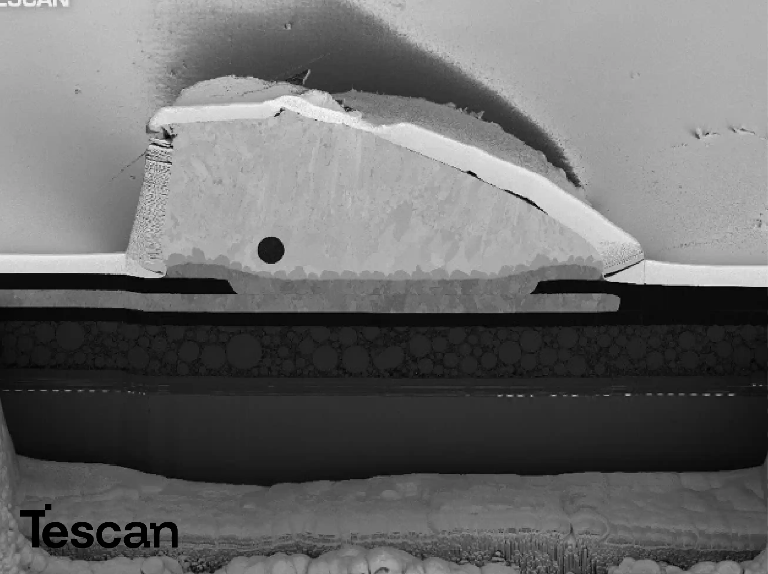
Tescan FIB-SEM systems allow researchers to target specific regions of interest within complex materials for precise cross-sectioning. Using a finely focused ion beam, the system can mill through surface layers with nanometer-scale accuracy, producing smooth, artifact-free sections. This capability is critical for analyzing multi-phase materials, composite interfaces, coatings, and microelectronic devices. Researchers can generate lamellae for further TEM or STEM analysis, enabling multi-scale characterization. The controlled ion beam minimizes mechanical stress and thermal damage, preserving the microstructural integrity while providing optimal surfaces for high-resolution imaging and quantitative analysis.
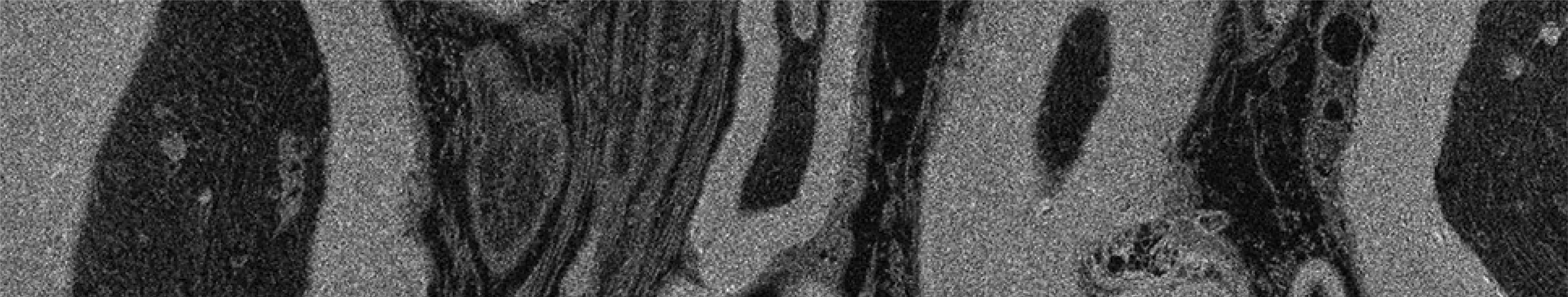
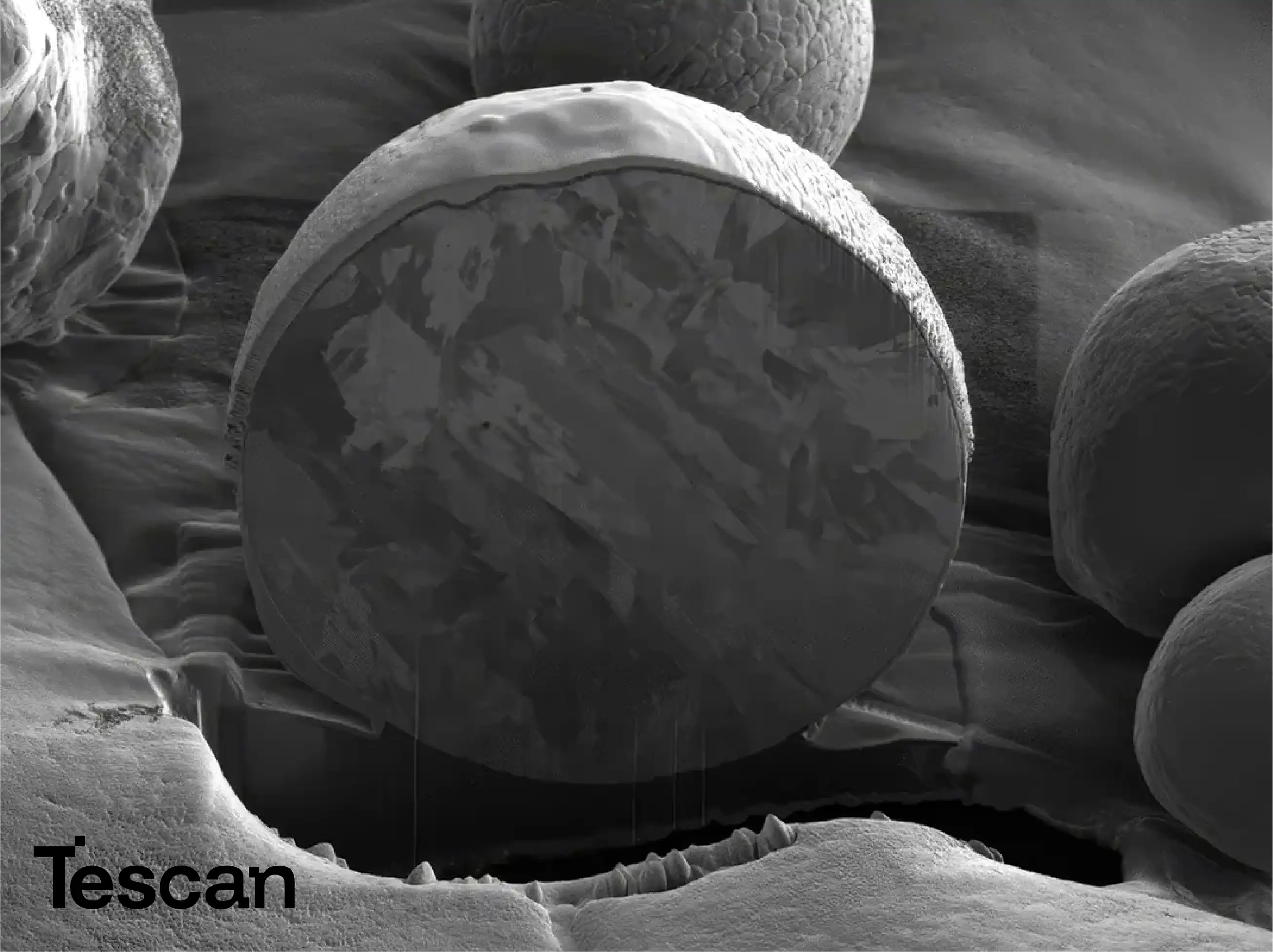
High-Resolution Imaging and Morphological Analysis
With advanced electron optics and optimized detectors, Tescan FIB-SEM systems deliver exceptional image resolution and contrast for diverse material types. Users can visualize grains, precipitates, pores, inclusions, and sub-micron defects with clarity, enabling quantitative morphological analysis. The platform provides stable beam conditions even for sensitive or irregular samples, allowing repeated imaging with minimal drift or distortion. This high-resolution capability is essential for understanding material behavior at the nanoscale, supporting research into fracture mechanisms, phase distribution, and interface morphology.
Three-Dimensional Tomography and Volumetric Reconstruction
The integration of automated ion milling and sequential SEM imaging allows Tescan FIB-SEM systems to generate volumetric reconstructions of material microstructures. Researchers can explore pore networks, cracks, and grain boundaries in three dimensions, revealing insights inaccessible to conventional 2D imaging. Volumetric datasets facilitate the quantification of internal microstructural features, including phase volume fractions, porosity, and connectivity. These 3D analyses are invaluable for understanding failure mechanisms, guiding material design, and validating computational models for both academic and industrial applications.
Analytical Integration for Composition and Crystallography
Tescan FIB-SEM systems can be coupled with analytical techniques such as energy-dispersive X-ray spectroscopy (EDS) and electron backscatter diffraction (EBSD). This integration provides simultaneous chemical, crystallographic, and structural information on the same sample region. Researchers can map elemental distributions across microstructural features, correlate phase composition with crystallographic orientation, and evaluate material heterogeneity. This combination is critical for alloy design, ceramics characterization, and semiconductor failure analysis, enabling a holistic understanding of materials.
Nanoscale Fabrication, Milling, and Microengineering
Beyond imaging, Tescan FIB-SEM systems offer capabilities for controlled material modification at the nanoscale. Focused ion beams can create precise micro- and nanostructures, modify interfaces, or deposit material in targeted areas. This functionality supports advanced device prototyping, semiconductor circuit inspection, and MEMS/NEMS fabrication. Users can perform multi-step workflows such as patterning, lift-out, and lamella preparation with accuracy and reproducibility, extending the platform’s utility from imaging and analysis to precise microengineering applications.
Automation, Workflow Optimization, and Reproducibility
Tescan FIB-SEM platforms feature advanced automation for repetitive and long-duration experiments. Automated milling, imaging, and 3D reconstruction workflows reduce operator variability and increase throughput. Intelligent pattern recognition and adaptive milling algorithms enable reliable serial sectioning for volumetric analysis across multiple samples. These automation features allow researchers to focus on data interpretation and quantitative analysis while ensuring consistent imaging quality, even in high-demand research or industrial environments.
Correlative Multi-Modal Microscopy
The versatility of Tescan FIB-SEM allows integration into correlative microscopy workflows. Users can combine optical, SEM, and ion beam data to identify regions of interest and conduct multi-scale analyses. This correlative approach ensures that nanoscale imaging is informed by macroscopic observations and contextual data, improving interpretation accuracy. Researchers can map microstructural features identified at lower resolution directly to high-resolution volumetric reconstructions, enabling comprehensive studies of structure–property relationships in materials science.
Broad Applications Across Material Science Fields
Tescan FIB-SEM systems are employed across a wide spectrum of material science disciplines, including metallurgy, ceramics, polymers, composites, semiconductors, and additive-manufactured materials. Applications include failure analysis, fracture mechanics, corrosion studies, interface characterization, and quality control. By combining high-resolution imaging, 3D reconstruction, and compositional analysis, these systems provide detailed insights into how microstructure influences material properties, supporting both fundamental research and industrial process optimization.
Read more about Tescan products here