
Nanoscale Chemical
|
Electronic Mapping using Integrated Microscopy
Horiba Microscopy and Imaging
The Microscopy and Imaging portfolio delivers advanced analytical solutions for characterizing material properties at spatial scales ranging from the micrometer down to the nanometer, fundamentally addressing the limitations of bulk analysis by providing site-specific chemical, structural, and electronic information. Core technologies such as Raman Microscopy and Cathodoluminescence enable non-destructive identification of molecular composition, crystal structure, stress, and semiconductor electronic band gaps.
This collection of analytical instruments is designed to overcome the persistent challenge of fully characterizing complex heterogeneous samples where a single method provides insufficient insight. For instance, coupling the high chemical specificity of Raman with the high spatial resolution of AFM allows researchers to directly correlate physical structures, defects, or nanoscale domains with their precise molecular composition, moving beyond simple size measurement to true functional mapping of advanced materials.
A key focus is on enhancing sensitivity and speed to improve sample throughput and minimize potential photodamage during acquisition. This is achieved through optimizing optical designs, employing high-efficiency detectors (like CCDs and InGaAs arrays), and integrating automated features like motorized stages and environmental control chambers. These design choices ensure that measurements—from long-duration Raman mapping acquisitions to temperature-dependent Cathodoluminescence studies, are performed rapidly, reliably, and under precise conditions necessary for generating actionable, high-quality analytical data.
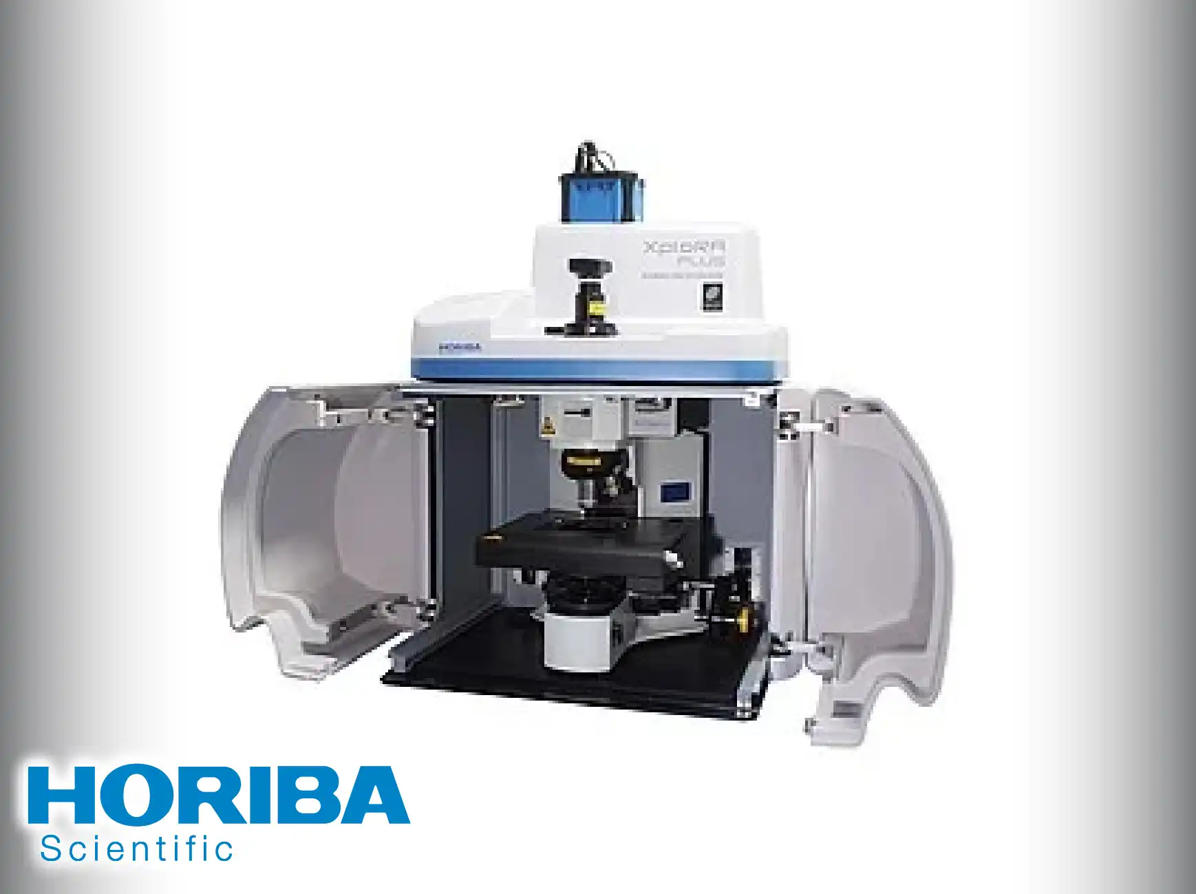
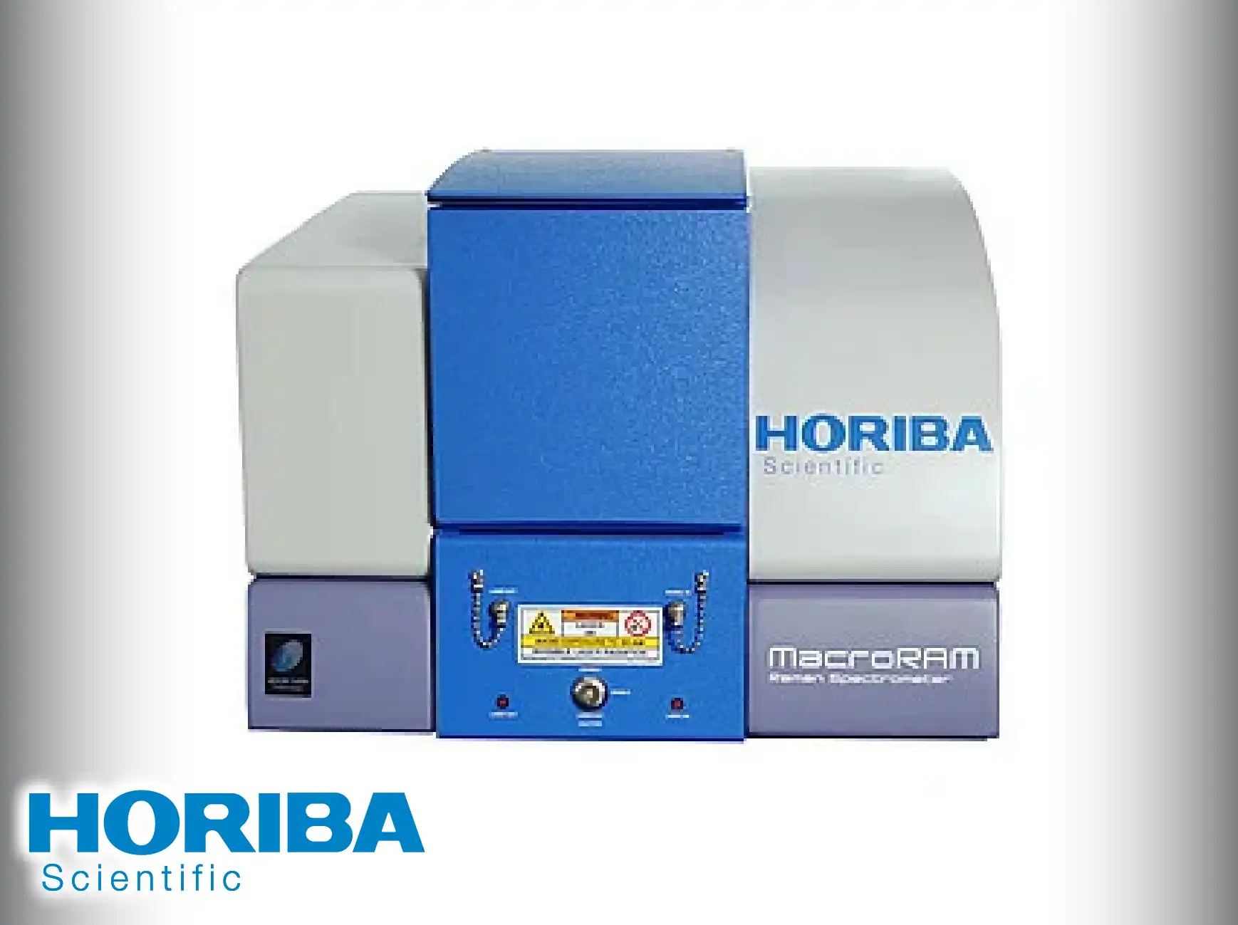
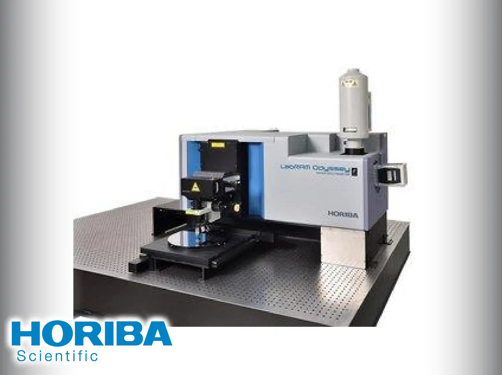
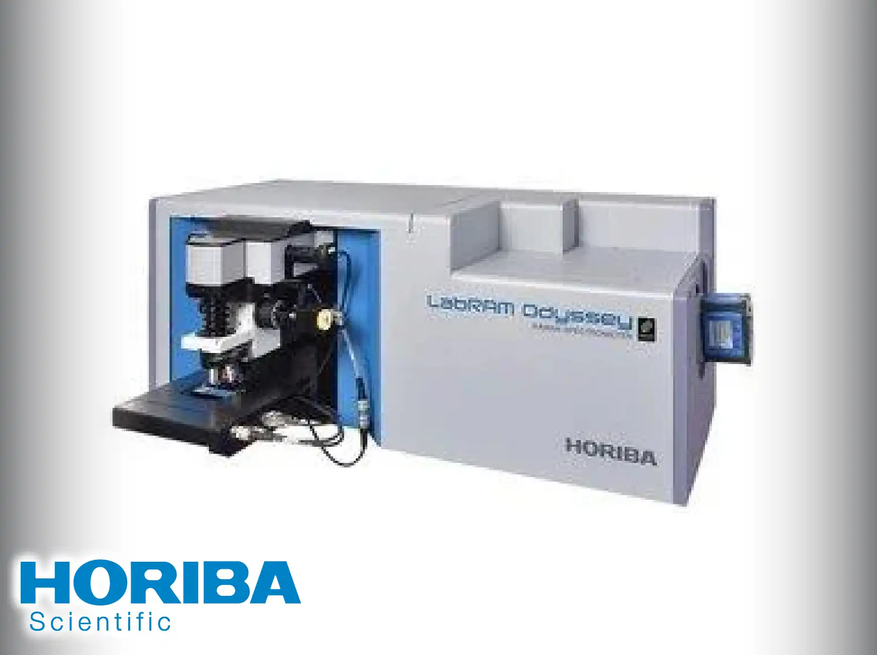
Raman Microscopy
- The technique provides non-destructive chemical fingerprinting by measuring the inelastic scattering of photons, which corresponds to the characteristic vibrational and rotational modes of molecules, resolving ambiguity in material identification across polymers, minerals, and pharmaceuticals.
- Integration with a confocal microscope enables sub-micrometer spatial resolution, allowing for detailed chemical mapping of heterogeneous materials by precisely focusing the laser spot and isolating the signal from the user-defined focal volume, eliminating depth-of-field confusion.
- Chemical distribution mapping is achieved by acquiring full Raman spectra across a defined sample area and processing the data to visualize the spatial arrangement and concentration gradients of different molecular components within the matrix.
- Specialized instrumentation allows for ultra-low wavenumber measurements (down to $5 \text{cm}^{-1}$), a capability essential for studying crystalline lattice dynamics, polymorph identification, and low-frequency vibrations in biological systems where these modes dictate material behavior.
- The system is capable of performing stress and strain analysis in materials like semiconductors or engineered coatings by precisely measuring the slight shifts in characteristic Raman peak positions, which directly correlate to mechanical deformation states.
- Implementation of polarization analysis enables the determination of molecular orientation and crystal symmetry within the sample, resolving structural details often obscured in isotropic measurements, especially vital for anisotropic films and fibers.
- High-stability optical benches and temperature-controlled detectors address the limitation of signal weakness inherent to the Raman effect, ensuring that long acquisition times necessary for low-concentration analysis are conducted without spectral drift or thermal noise corruption.
- Automated high-speed motorized stages and advanced software algorithms significantly reduce the time required for comprehensive area mapping, enabling high-throughput chemical analysis of large samples without sacrificing spatial resolution.
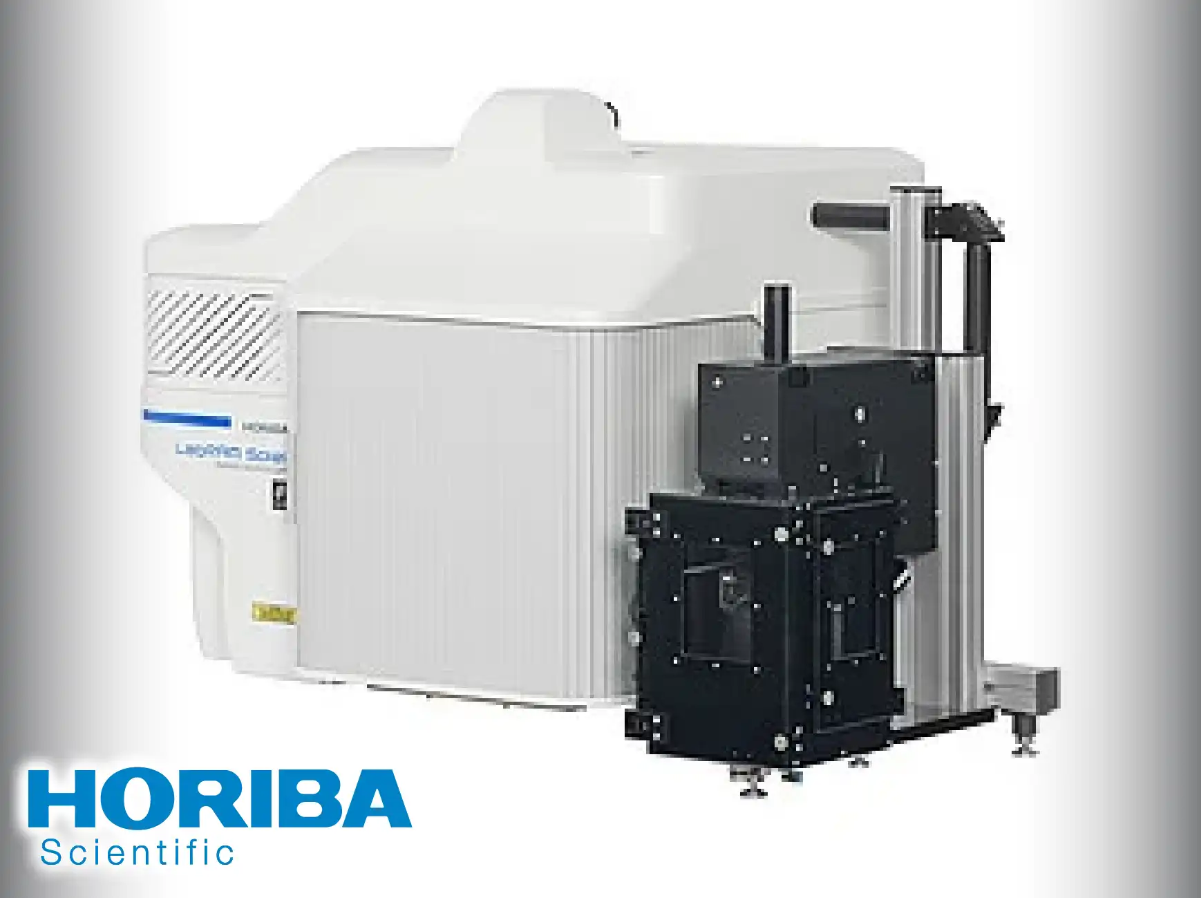
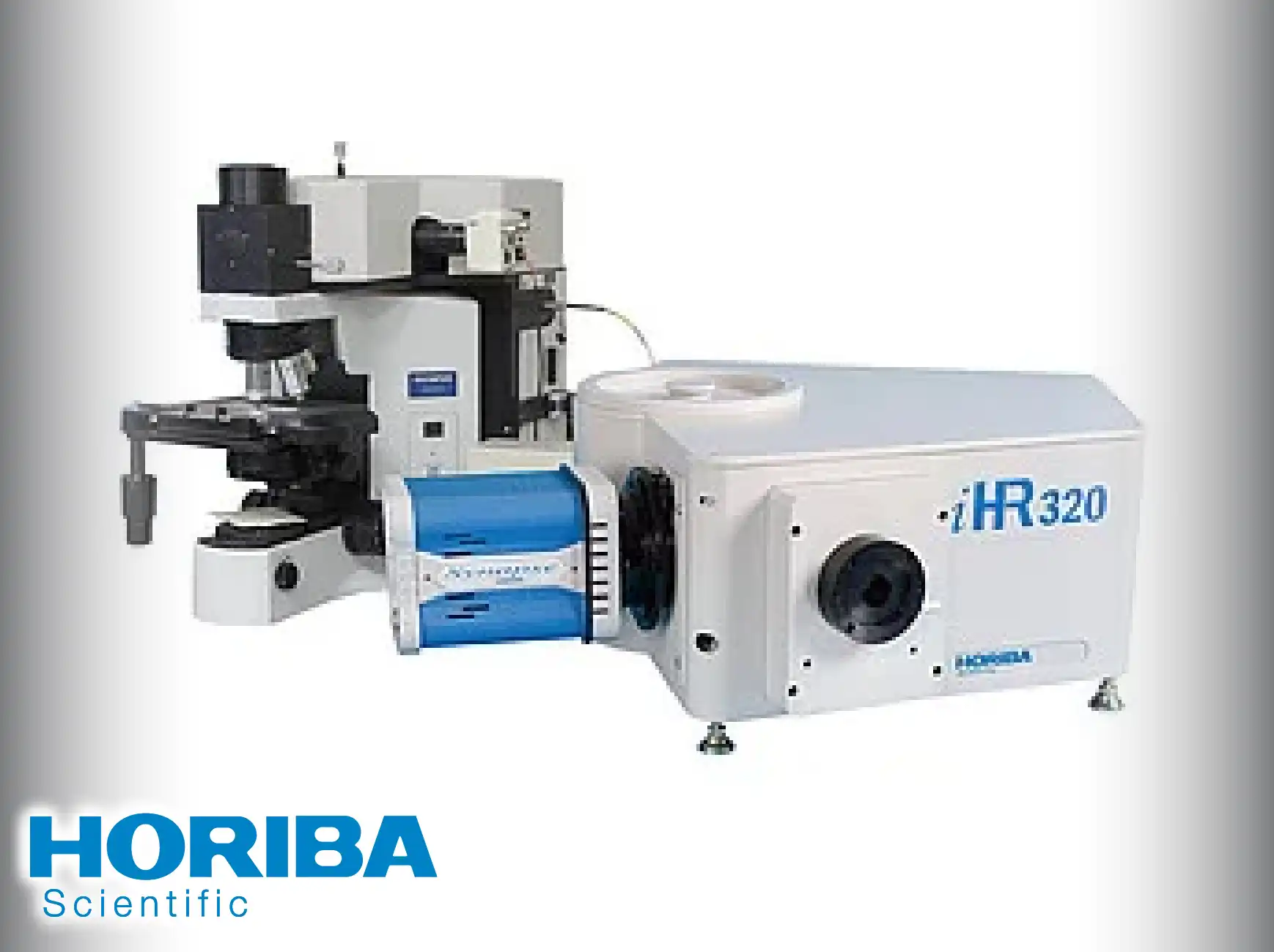
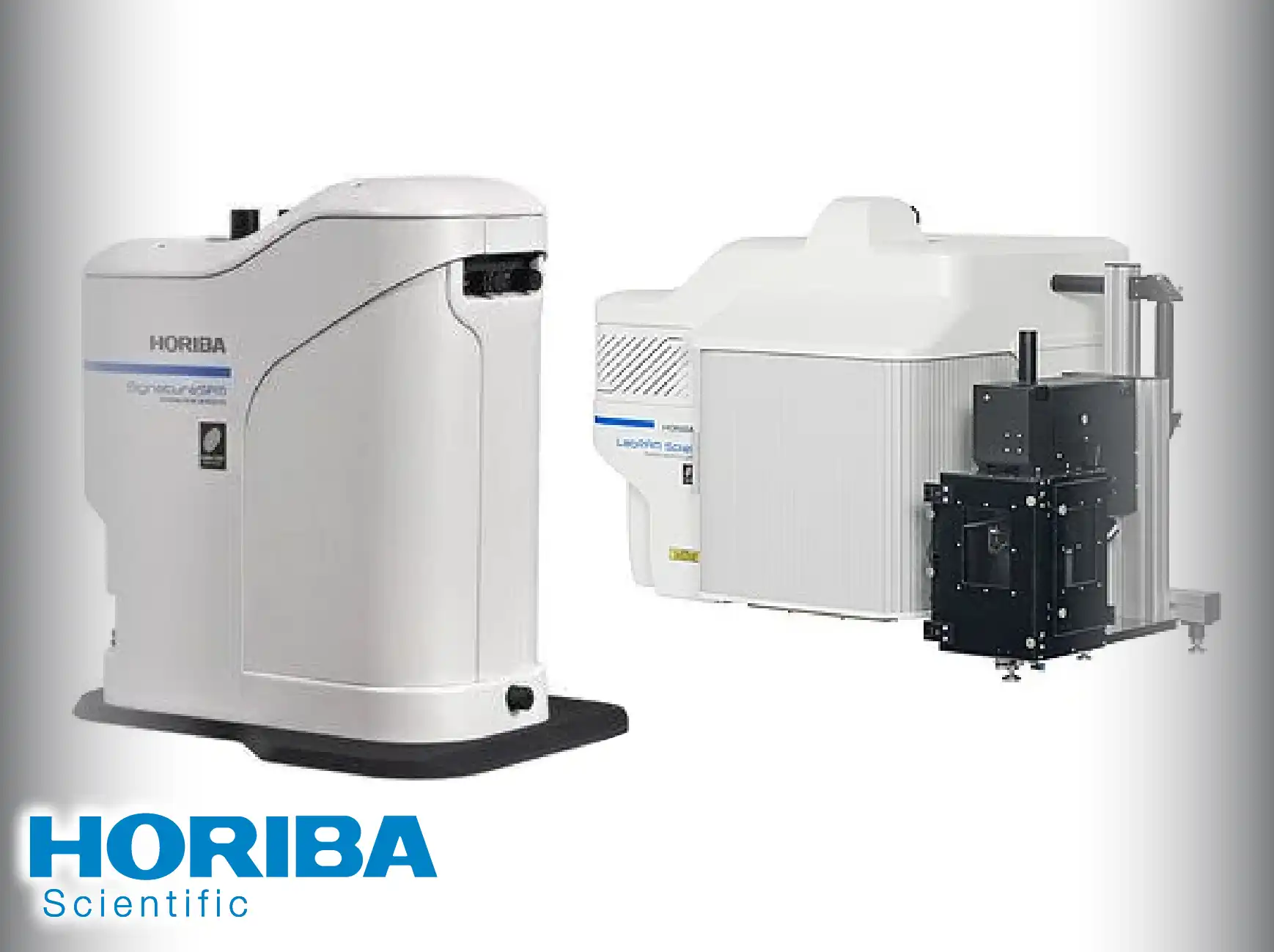
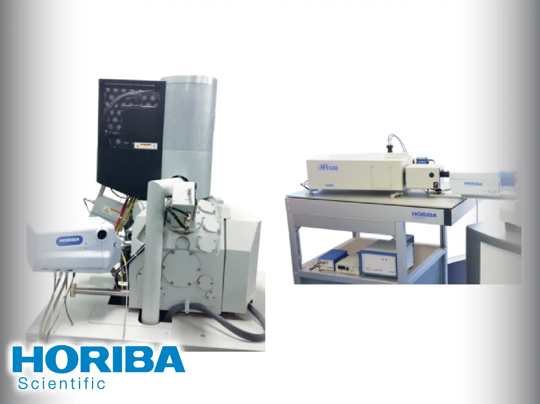
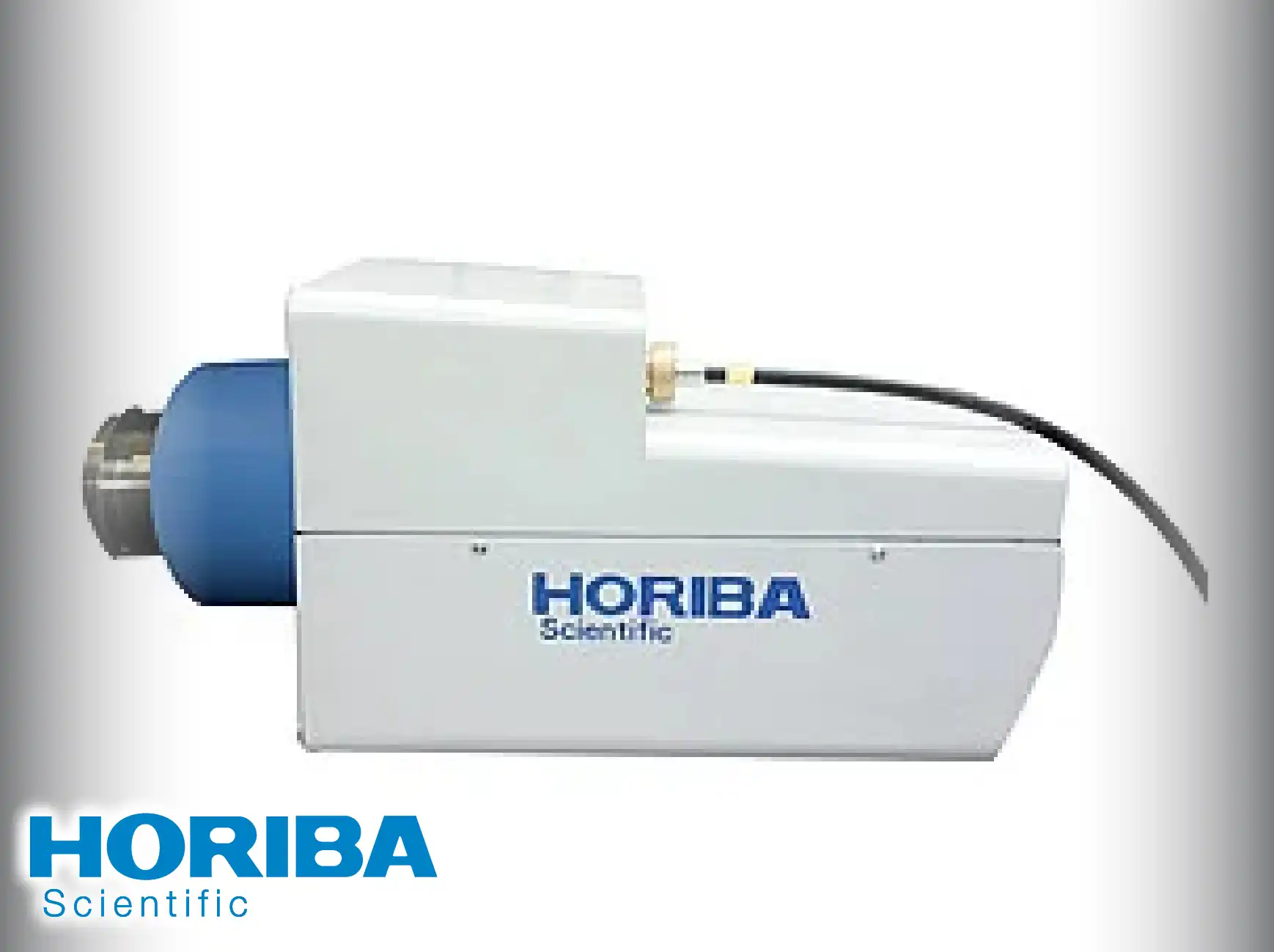
Cathodoluminescence (CL)
- CL provides access to the electronic and optical properties of materials, such as semiconductors and ceramics, by analyzing the light emitted when the material is excited by a high-energy electron beam within a Scanning Electron Microscope (SEM) chamber.
- The electron beam excitation source inherently overcomes the diffraction limit of light, allowing for spatial resolution in the nanoscale range (sub-100 nm), which is critical for mapping defects and band structure variations in microelectronic devices.
- The spectral analysis capability allows researchers to precisely determine the electronic band gap of materials and map local variations in crystal quality or dopant concentration, which directly influence device performance.
- CL is a crucial tool for defect characterization in wide-bandgap semiconductors (e.g., GaN, SiC) and geological samples, visualizing non-radiative defects and impurities that are otherwise invisible using standard structural imaging techniques.
- The integration requires specialized optics within the vacuum chamber (e.g., parabolic mirror or lens collection systems) to efficiently capture the emitted light across a wide spectral range (UV, Visible, NIR) and transfer it to the spectrometer and detector.
- Systems often incorporate cryogenic cooling stages (e.g., to 77 K or lower) to suppress thermal broadening of spectral peaks, enabling the resolution of subtle excitonic features and improving the signal-to-noise ratio for precise quantitative analysis.
- The technique provides unique information on local optical anisotropy and dipole orientation through specialized polarization measurements of the emitted CL light, offering structural insight at the nanoscale beyond basic composition.
- The ability to correlate the CL signal directly with high-magnification SEM topography (using integrated sample alignment) ensures that observed spectral features can be definitively localized to specific physical structures or interfaces on the sample surface.
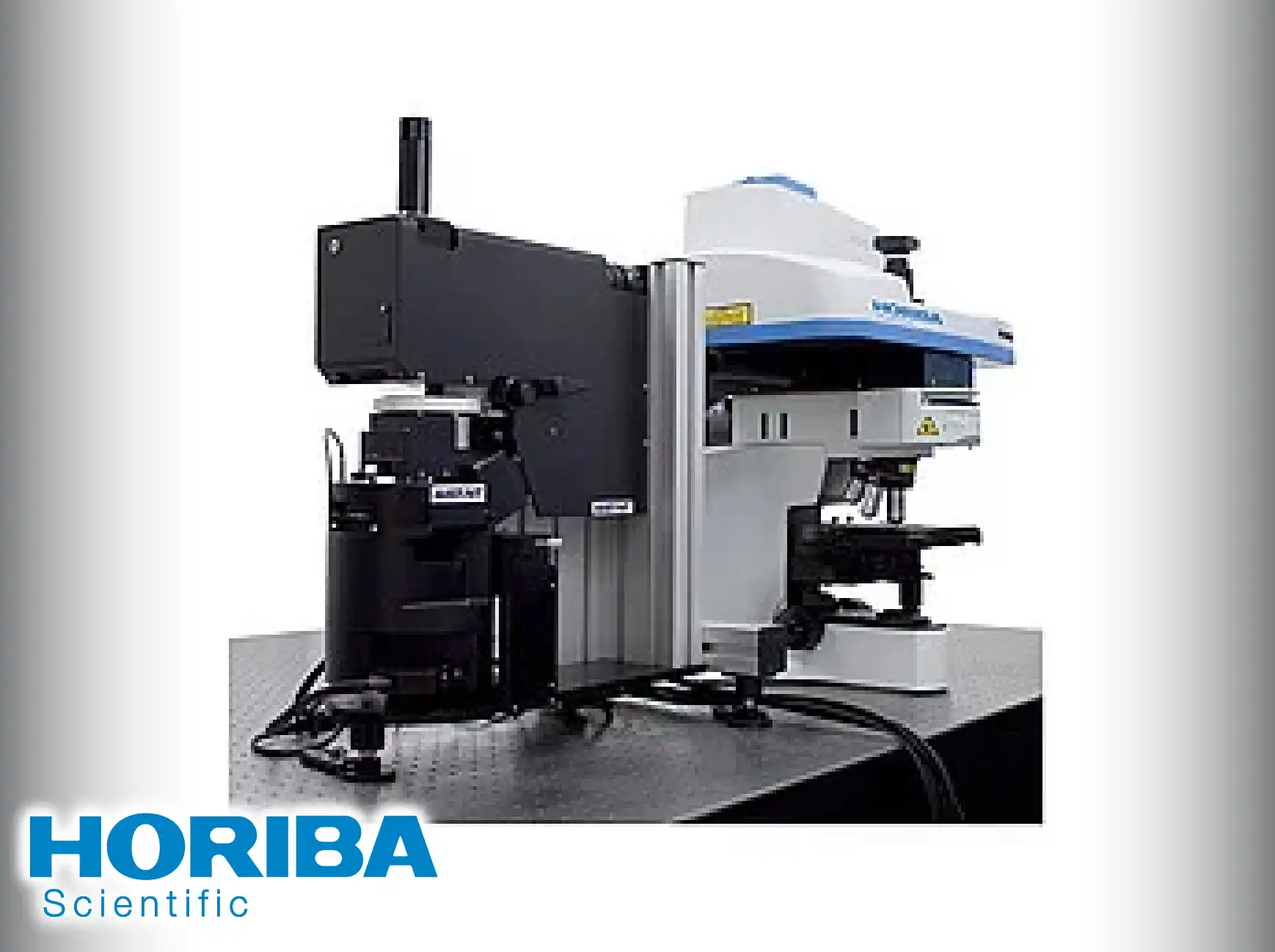
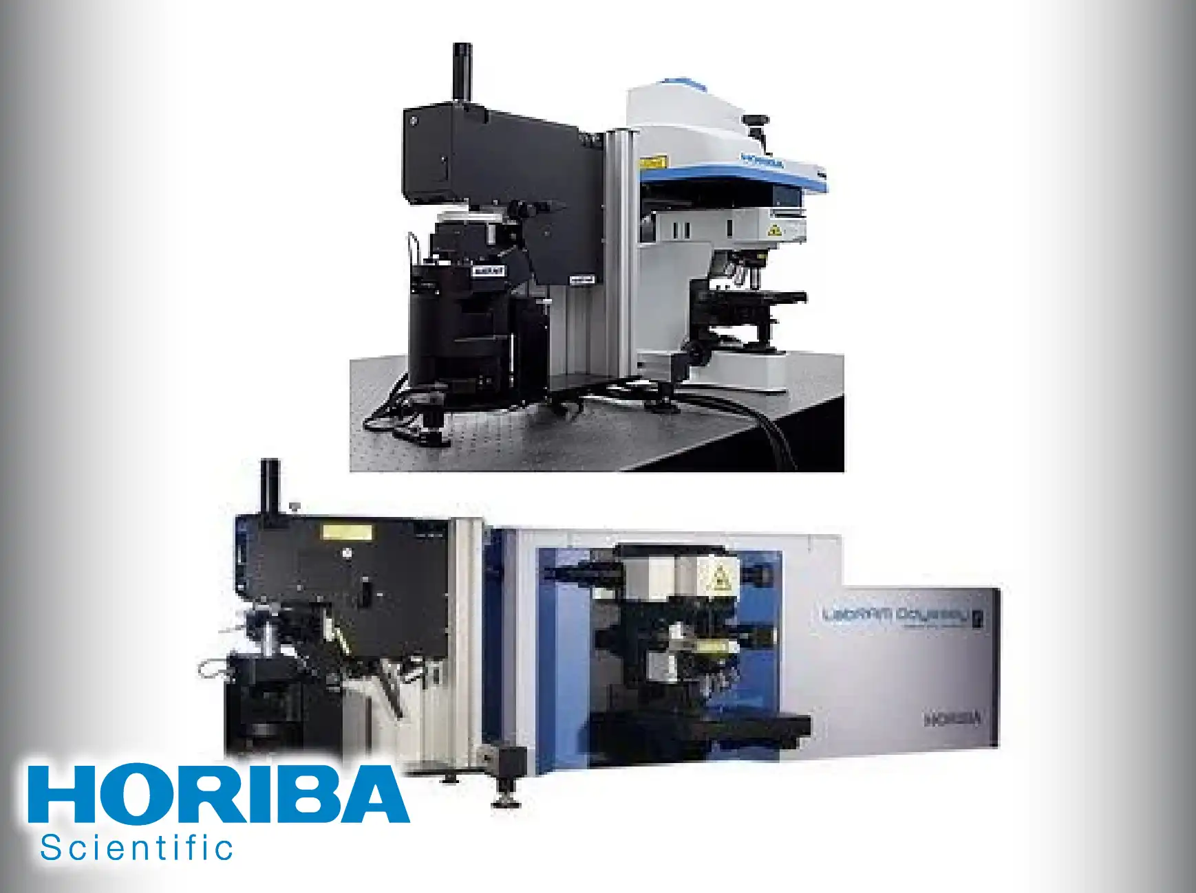
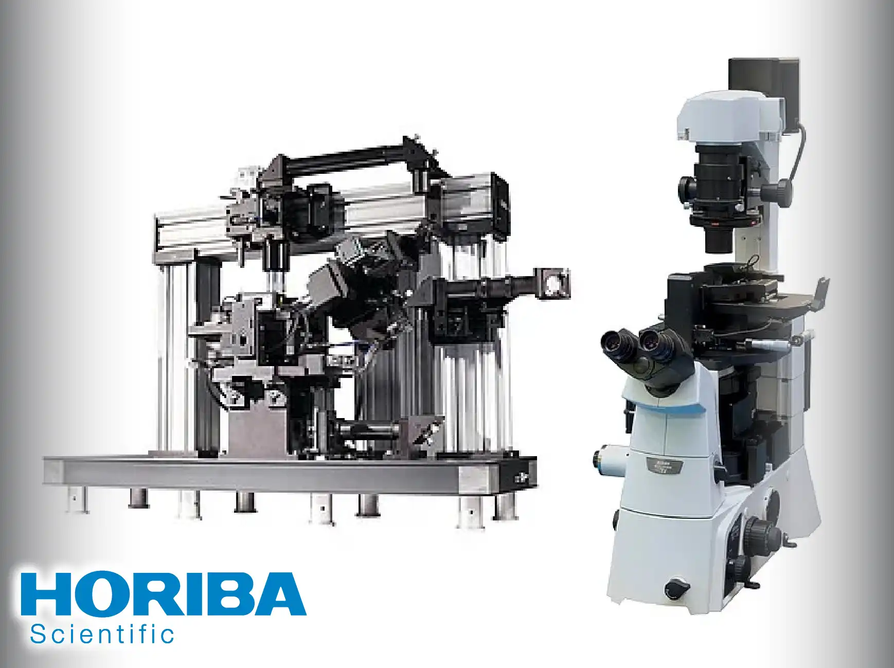
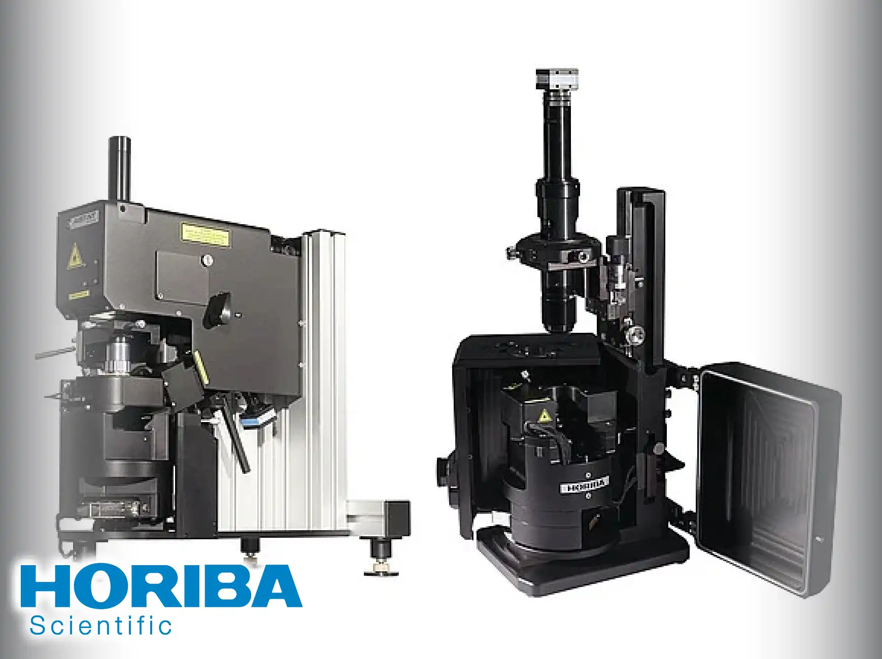
AFM-Raman Integration
- The primary advantage is the combination of high-resolution topographical imaging (AFM) with molecular specificity (Raman), resolving the challenge of correlating a material's physical morphology (roughness, height) with its chemical makeup at the same exact point.
- The integrated system enables Tip-Enhanced Raman Spectroscopy (TERS), where a plasmon-generating AFM tip acts as an optical antenna, overcoming the diffraction limit and achieving chemical resolution down to the nanometer scale.
- TERS allows for single-molecule sensitivity or the analysis of incredibly small domains, addressing the limitation of conventional Raman which requires a bulk volume of material to produce a detectable signal.
- The AFM component provides accurate force spectroscopy measurements alongside chemical analysis, enabling the simultaneous study of a sample’s local mechanical properties (stiffness, adhesion) and its chemical identity.
- The ability to operate in various AFM modes (e.g., contact, tapping, non-contact) ensures optimal force control and sample preservation while the chemical data is acquired, which is critical for delicate biological or polymeric samples.
- Specialized closed-loop feedback mechanisms are vital for maintaining the nanometric distance between the TERS tip and the sample surface during chemical mapping, ensuring the maximal plasmonic enhancement necessary for high-fidelity TERS data.
- The platform addresses the critical alignment challenge by using integrated optical viewing and precise motorized positioning, allowing the user to align the focused laser, the TERS tip, and the measurement area with sub-micron precision.
- Environmental control options (e.g., heating/cooling stages, humidity control) permit the study of dynamic chemical changes in situ—such as phase transitions or reaction kinetics—while retaining the high spatial resolution of the AFM-Raman technique.
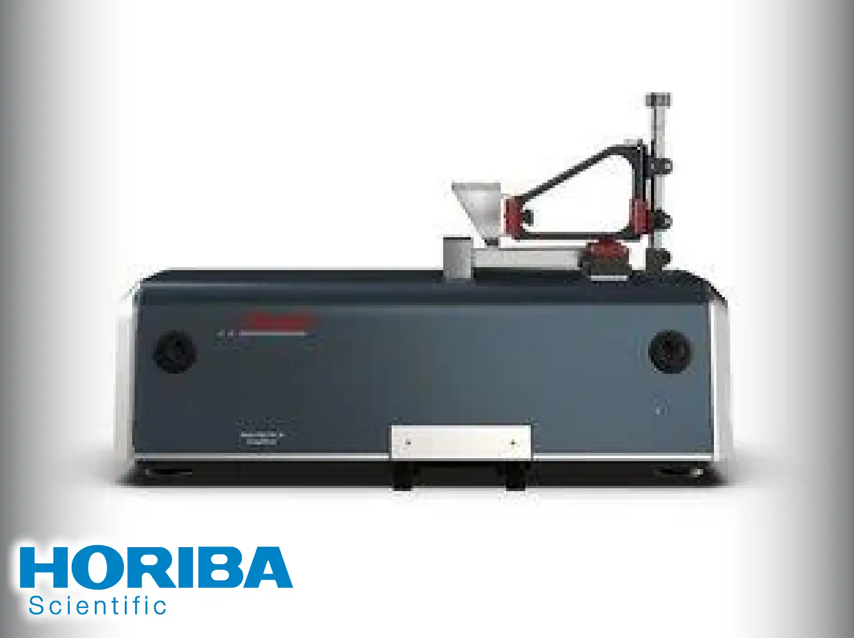
Nanoparticle Tracking Analysis (NTA)
- NTA provides a size distribution based on the direct visualization and individual tracking of nanoparticles, fundamentally overcoming the averaging artifacts inherent in ensemble techniques like DLS, especially for highly polydisperse samples.
- The instrument captures a video of nanoparticles undergoing Brownian motion, allowing the software to calculate the diffusion coefficient and subsequently the hydrodynamic diameter for each particle independently, leading to higher resolution distributions.
- The visualization capability addresses the need for real-time kinetic monitoring; analysts can observe changes in size distribution, aggregation, or dissolution as they occur, providing direct, qualitative evidence to support quantitative data.
- NTA delivers absolute particle concentration ($particles/mL$) by counting the number of tracked particles within a defined field of view and volume, which is essential for accurate dosing in therapeutic applications and yield calculation in synthesis.
- The use of laser illumination and optimized optics creates a high-contrast environment, ensuring that even weakly scattering, small nanoparticles (down to $10 \text{nm}$) are clearly visible against the background, resolving the challenge of detecting the lowest size fraction.
- The technology is highly effective for characterizing complex biological matrices, such as extracellular vesicles or viral particles, providing key metrics (size, count, fluorescence labeling) without requiring extensive, potentially damaging, sample pre-treatment.
- By employing fluorescence mode, NTA can specifically track and count subsets of labeled particles within a complex mixture, solving the problem of analyzing low-concentration functionalized particles amidst high concentrations of non-labeled background material.
- The measurement process is relatively fast and calibration-free, relying solely on the viscosity and temperature of the medium, which simplifies the analytical workflow and ensures faster, more reproducible results compared to methods requiring reference standards.
Click here for more information about Horiba Solutions