.jpg)
Home » Products » Scanning Electron Microscopy » Focused Ion Beam-Scanning Electron Microscopes (FIB-SEM)
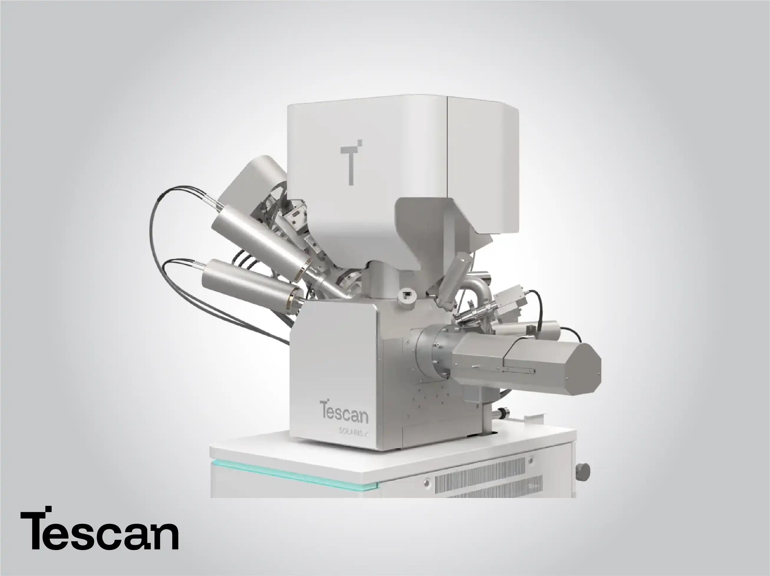
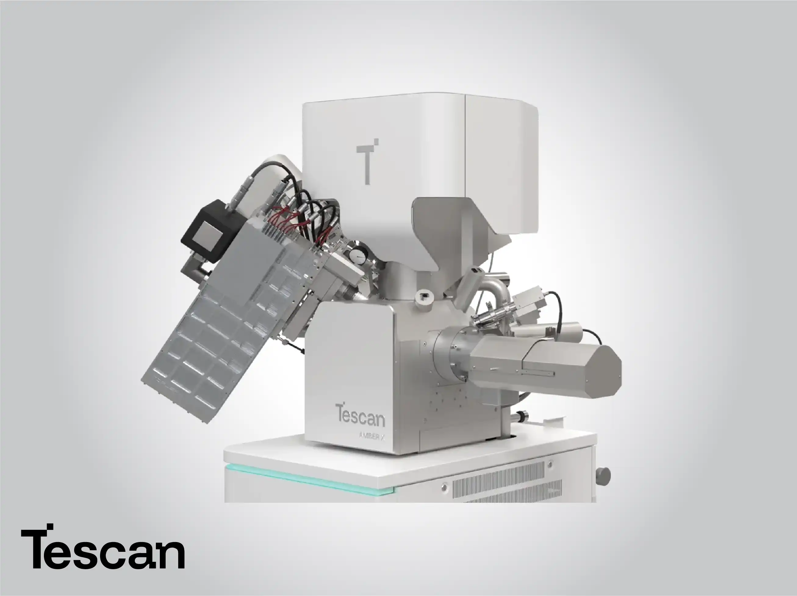
Advanced Focused Ion Beam
|
(FIB-SEM) for Precision Nanofabrication and Analysis
Home » Products » Scanning Electron Microscopy » Focused Ion Beam-Scanning Electron Microscopes (FIB-SEM)
(FIB-SEM) for Precision Nanofabrication and Analysis